Part Number: CDCEL913
Other Parts Discussed in Thread: SN65DSI83-Q1, , SN65DSI83, CDCE913
Tool/software:
Dear Expert,
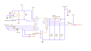
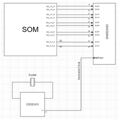
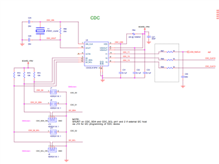
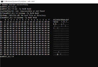
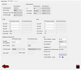
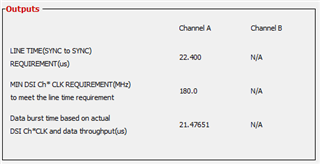
We are currently utilizing the SN65DSI83-Q1 as our LVDS converter. However, we have encountered issues with noise and jitter in the clock signal generated from the SOM. To address this, we have decided to implement the CDCEL913 Clock Generator as an external reference clock. Enclosed are the block diagram and schematic for the clock generator.
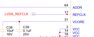
Could you please advise if a pull-up resistor is necessary for the LVDS_REFCLK? Additionally, are there any other modifications required for our design?
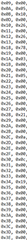
We are also experiencing a PLL unlock message in the SN65DSI83, which is resulting in the output being turned off.
Thank you,
Adarsh Verma