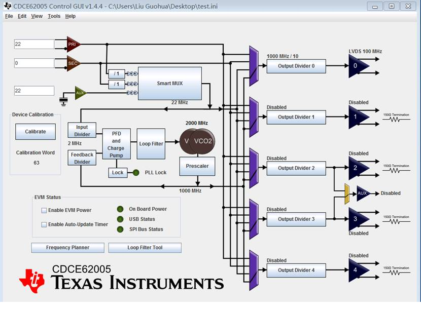
This thread has been locked.

If you have a related question, please click the "Ask a related question" button in the top right corner. The newly created question will be automatically linked to this question.

cdce62005 can't lock

Other Parts Discussed in Thread: CDCE62005


I used the CDCE62005 Controller GUI v1.4.4" generate a register value, then I configure them 

through SPI , the read back vaule of every register is right(same as the write data),

but It can't lock anyway, is there any error or whether the chip is out of work?

                                                                                                     thanks 

(I don't use 62005EVM board ,but a board designed by myself.)


REGISTERS

0 eb0603ef

1 68ffffff

2 68ffffcf

3 68ffffef

4 68ffffff

5 fc2bff3f

6 efffc9ef

7 fd183e0f

8 ffffffff


PORTS

0 bf

1 ff

2 df

3 f9


INPUTS

PRI 22

SEC 0

AUX 22


EXTERNAL COMPONENTS

C4 4.7E-06

R4 1000

C5 2.7E-07

  • another question:

    when I configure the registers through SPI, what's the right sequence?


    1.  reg0->reg1->......->reg7     or

    2.  reg7->reg6->......->reg0    


                                                      Thanks

  • Hi Guohua,

    your register values seem completely wrong - they should have the register value from 0-8 at the end.

    Here is my recommendation:

    REGISTERS

    Register settings:
    0 eb060320
    1 68860301
    2 68060302
    3 680e0303
    4 680e0334
    5 10280a75
    6 1cf49e6
    7 bd927bf7
    8 80009818

    PORTS
    0 dd
    1 ff
    2 df
    3 f9

    INPUTS
    PRI 22
    SEC 0
    AUX 22

    EXTERNAL COMPONENTS
    C4 1
    R4 1
    C5 1

    This setting would expect a differential, AC-coupled signal on PRI_IN. The secondary input is disabled.

    By the way, you can always check if the input buffer works, if you go to any of the output muxes and select to bring out the primary input. This way you can be sure you actually receive the 22MHz signal.

    Concerning the loop filter:

    Use 2.5mA charge pump current and set the internal loop filter with C1=23pF, R2=9k, C2=473.5pF, R3=5k, and C3=5.5pF as a starting point. This setting should give you 62 degree phase margin, 232k loop bandwidth, and a Gamma of two, which should be a good start.

    stand-alone loop filter tool (calculates Gamma):

    integrated loop filter tool (gamma not re-calculated):


    Concerning Calibration:

    The sequence whether to write register 0 to 7 or 7 to 0 is no important. What matters is that all output become re-syncronized and the VCO calibrated.

    For SYNC, check out register 8 bit 8 definition. SYNC is actually generated anytime you change an output divider setting, so you can ignore toggling R8.8 in your initialization sequence unless your output phase need to have a particular phase relationship with the input clock or other sync in the system.

    Most importantly, you need to initiate calibration - otherwise your VCO will stay unlocked. You need to start calibration AFTER your input signal is valid (e.g. after the 22MHz are available).

    I suggest you look at data sheet table 46 to identify one of two potential methods for calibration:


    While calibration occurs, the outputs will be turned off. After calibration, the outputs turn on immediately.

    Best regards, Fritz