This thread has been locked.

If you have a related question, please click the "Ask a related question" button in the top right corner. The newly created question will be automatically linked to this question.

LP-MSPM0G3507: LP-MSPM0G3507

Part Number: LP-MSPM0G3507
Other Parts Discussed in Thread: MSPM0G3507, SYSCONFIG

Tool/software:

Hi everyone,

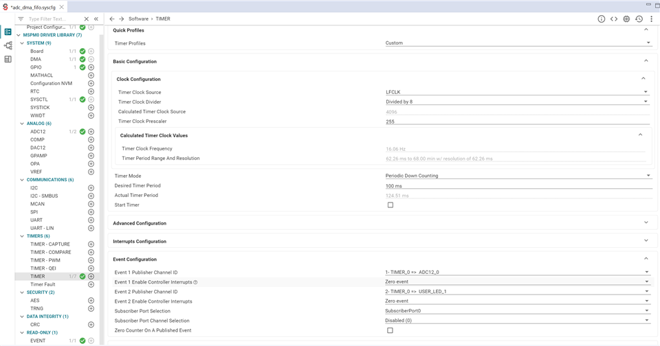
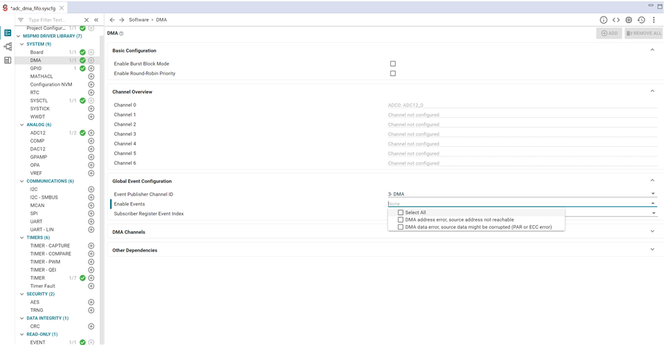
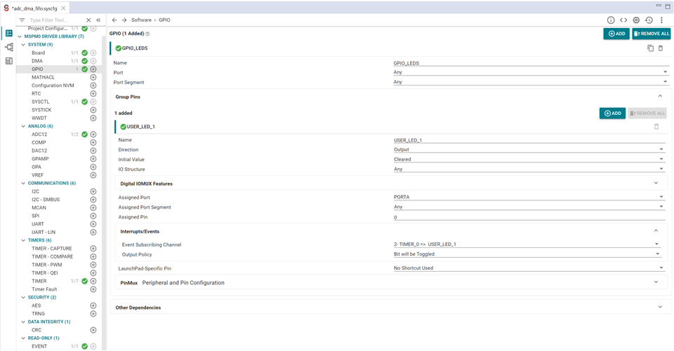
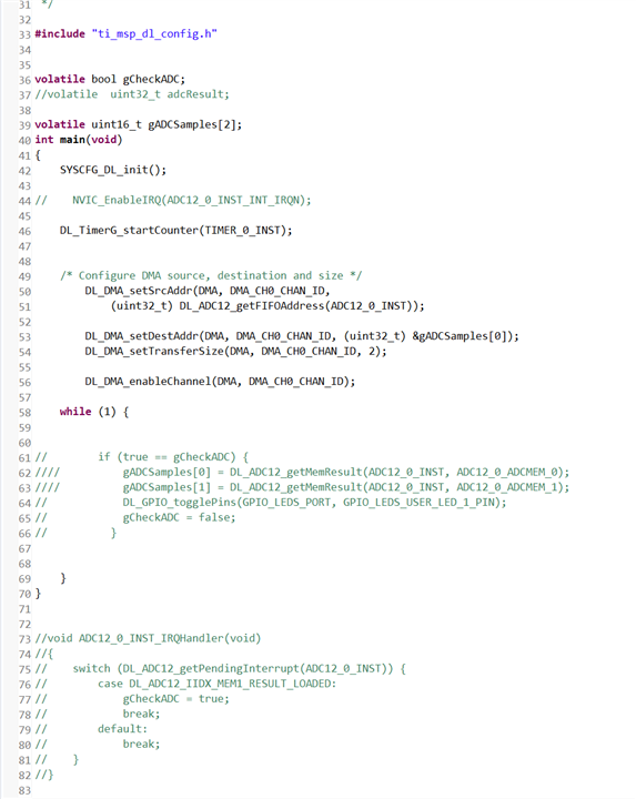
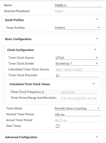
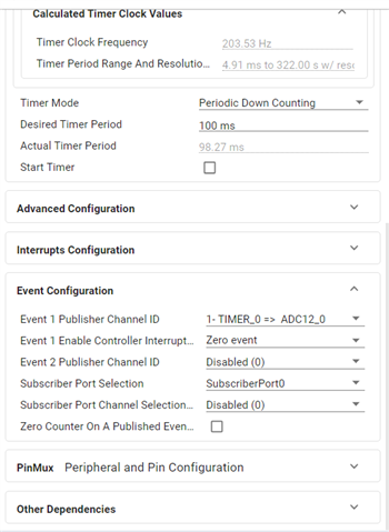
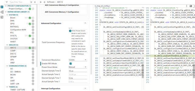
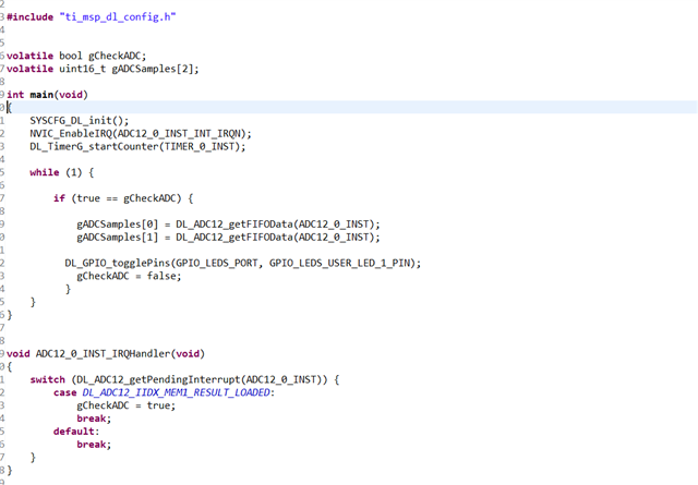
I am currently working on a project where I am using DMA and FIFO for data transfer and have encountered an issue with timing. Previously, I read multiple channels without DMA and FIFO, and the LED toggled at an expected rate after completing the read operations. However, after enabling FIFO and DMA, the LED toggle has become noticeably slower.

I am trying to understand the cause of this slowdown. Could the configuration of DMA and FIFO affect the data transfer speed negatively? Are there specific settings or considerations I might be overlooking that could improve the timing?

Thank you for your support!

Best regards,

Ali

  • Hi Ali,

    Are you using one of the FIFOs for one of our peripherals, like UART/I2C/SPI, or are you using a software FIFO that you've created on your own?

    Also, what mechanism are you using to toggle the LED with your new DMA + FIFO implementation? Are you certain that you are toggling on the same action that you were before without the DMA + FIFO?

    I ask because generally speaking, utilizing DMA should cause your data transfers to be at least the same speed if not faster. I suspect something in your implementation is causing the delay, or the appearance of one.

  • I am using the FIFO in the  ADC  adc12->ULLMEM.CTL2 |= (ADC12_CTL2_FIFOEN_ENABLE);

    I am trying to do something similar to adc12_max_freq_dma_LP_MSPM0G3507_nortos_ticlang project but using muliple channels 

    for toggling mechansim every time the ADC12_IIDX_DMA_DONE Flag is set the LED is toggled 

  • So I assume that the DMA is triggered on one of the MEMx result loaded flags, then you have the DMA channel publish an event, to which the GPIO is subscribed? Or the DMA done flag is being used as an interrupt and the LED is toggled with software? 

    Is it possible that the DMA is transferring all of the ADC conversion data at once, so now you are only seeing the LED toggle when all x (not sure how many channels you are converting on) channels have completed their conversion and DMA transfer, whereas before you were toggling on every channels completed transfer? 

    It may be helpful to expand your Sysconfig tabs (if you are using it) and posting images here. Otherwise a code snippet may help as well.

  • "So I assume that the DMA is triggered on one of the MEMx result loaded flags, then you have the DMA channel publish an event, to which the GPIO is subscribed?"

    No I use a timer as a publisher and an ADC as a subscriber then I check the flag of the ADC if it DL_ADC12_IIDX_DMA_DONE when so I set a flag as true and toggle a LED in the while(1) loop. The timer trigger the ADC every 100 ms it was correct when I use one channel or multiple channel without DMA and in this case i checked  the DL_ADC12_IIDX_MEM1_RESULT_LOADED flag.

    When the DMA transfers the data then i checked the DL_ADC12_IIDX_DMA_DONE  flag and the timing was not accurate. 

    I tryed now in code composer to do a publisher subscriber between DMA channel 0 and GPIO Pin PA0 but I can not do that unfortunatly.

    Best regards,

  • Looking over these I am primarily wondering if the DMA is set up correctly, especially since the configuration is not working at this point.

    In the ADC12 tab in Sysconfig there is a DMA configuration tab that will make this a bit easier, maybe that was how you did it before.

    Additionally, looking over these settings, it looks like the timer entirely determines the frequency of the LED blinking. I would not expect DMA additions to change the frequency at all here. Unless you've changed the timer settings as well, or the system clock settings, the LED frequency should not change. 

    I also do not see where you check the DMA done flag or its timing so I am not clear on how you are checking this timing. 

    Please let me know if I am missing something here or if you have further information. Thanks

  • I think it has to do with FIFO, because now I am only using the the timer G0, which triggers the adc every 100 ms when I disable the FIFO then the timing of toggle the LED is correct 100ms, but when I enable the FIFO then the Timing of the toggling the LED is not correct


  • Moreover I am only using two channels

  • Originally, you had the Timer publishing to the ADC and to the LED, so the ADC behavior would not affect the LED blinking rate, only the timer would. 

    In the most recent screenshot you are no longer using the timer to publish to the LED, so which event is publishing to it? If you change your settings please show me all of the settings so I can see how these pieces connect.

    Please check what signal you use to trigger the LED, and which event you are using to empty the ADC FIFO using the DMA, as this may illuminate why the LED is toggling slower. These should all be shown in Sysconfig. I'd also recommend configuring the DMA inside of the ADC tab so that some of these settings are completed for you.

    My suspicion is that the trigger to toggle the LED is occurring once per set of ADC conversions, rather than once per conversion, making the LED toggle slower despite a higher data rate.

  • /*
     * Copyright (c) 2023, Texas Instruments Incorporated
     * All rights reserved.
     *
     * Redistribution and use in source and binary forms, with or without
     * modification, are permitted provided that the following conditions
     * are met:
     *
     * *  Redistributions of source code must retain the above copyright
     *    notice, this list of conditions and the following disclaimer.
     *
     * *  Redistributions in binary form must reproduce the above copyright
     *    notice, this list of conditions and the following disclaimer in the
     *    documentation and/or other materials provided with the distribution.
     *
     * *  Neither the name of Texas Instruments Incorporated nor the names of
     *    its contributors may be used to endorse or promote products derived
     *    from this software without specific prior written permission.
     *
     * THIS SOFTWARE IS PROVIDED BY THE COPYRIGHT HOLDERS AND CONTRIBUTORS "AS IS"
     * AND ANY EXPRESS OR IMPLIED WARRANTIES, INCLUDING, BUT NOT LIMITED TO,
     * THE IMPLIED WARRANTIES OF MERCHANTABILITY AND FITNESS FOR A PARTICULAR
     * PURPOSE ARE DISCLAIMED. IN NO EVENT SHALL THE COPYRIGHT OWNER OR
     * CONTRIBUTORS BE LIABLE FOR ANY DIRECT, INDIRECT, INCIDENTAL, SPECIAL,
     * EXEMPLARY, OR CONSEQUENTIAL DAMAGES (INCLUDING, BUT NOT LIMITED TO,
     * PROCUREMENT OF SUBSTITUTE GOODS OR SERVICES; LOSS OF USE, DATA, OR PROFITS;
     * OR BUSINESS INTERRUPTION) HOWEVER CAUSED AND ON ANY THEORY OF LIABILITY,
     * WHETHER IN CONTRACT, STRICT LIABILITY, OR TORT (INCLUDING NEGLIGENCE OR
     * OTHERWISE) ARISING IN ANY WAY OUT OF THE USE OF THIS SOFTWARE,
     * EVEN IF ADVISED OF THE POSSIBILITY OF SUCH DAMAGE.
     */

    /*
     *  ============ ti_msp_dl_config.c =============
     *  Configured MSPM0 DriverLib module definitions
     *
     *  DO NOT EDIT - This file is generated for the MSPM0G350X
     *  by the SysConfig tool.
     */

    #include "ti_msp_dl_config.h"

    /*
     *  ======== SYSCFG_DL_init ========
     *  Perform any initialization needed before using any board APIs
     */
    SYSCONFIG_WEAK void SYSCFG_DL_init(void)
    {
        SYSCFG_DL_initPower();
        SYSCFG_DL_GPIO_init();
        /* Module-Specific Initializations*/
        SYSCFG_DL_SYSCTL_init();
        SYSCFG_DL_TIMER_0_init();
        SYSCFG_DL_ADC12_0_init();
    }


    SYSCONFIG_WEAK void SYSCFG_DL_initPower(void)
    {
        DL_GPIO_reset(GPIOA);
        DL_GPIO_reset(GPIOB);
        DL_TimerG_reset(TIMER_0_INST);
        DL_ADC12_reset(ADC12_0_INST);

        DL_GPIO_enablePower(GPIOA);
        DL_GPIO_enablePower(GPIOB);
        DL_TimerG_enablePower(TIMER_0_INST);
        DL_ADC12_enablePower(ADC12_0_INST);
        delay_cycles(POWER_STARTUP_DELAY);
    }

    SYSCONFIG_WEAK void SYSCFG_DL_GPIO_init(void)
    {

        DL_GPIO_initDigitalOutput(GPIO_LEDS_USER_LED_1_IOMUX);

        DL_GPIO_clearPins(GPIO_LEDS_PORT, GPIO_LEDS_USER_LED_1_PIN);
        DL_GPIO_enableOutput(GPIO_LEDS_PORT, GPIO_LEDS_USER_LED_1_PIN);

    }


    SYSCONFIG_WEAK void SYSCFG_DL_SYSCTL_init(void)
    {

        //Low Power Mode is configured to be SLEEP0
        DL_SYSCTL_setBORThreshold(DL_SYSCTL_BOR_THRESHOLD_LEVEL_0);

        DL_SYSCTL_setSYSOSCFreq(DL_SYSCTL_SYSOSC_FREQ_BASE);
        /* Set default configuration */
        DL_SYSCTL_disableHFXT();
        DL_SYSCTL_disableSYSPLL();
        DL_SYSCTL_setULPCLKDivider(DL_SYSCTL_ULPCLK_DIV_1);
        DL_SYSCTL_setMCLKDivider(DL_SYSCTL_MCLK_DIVIDER_DISABLE);

    }


    /*
     * Timer clock configuration to be sourced by LFCLK /  (4681.142857142857 Hz)
     * timerClkFreq = (timerClkSrc / (timerClkDivRatio * (timerClkPrescale + 1)))
     *   203.527950310559 Hz = 4681.142857142857 Hz / (7 * (22 + 1))
     */
    static const DL_TimerG_ClockConfig gTIMER_0ClockConfig = {
        .clockSel    = DL_TIMER_CLOCK_LFCLK,
        .divideRatio = DL_TIMER_CLOCK_DIVIDE_7,
        .prescale    = 22U,
    };

    /*
     * Timer load value (where the counter starts from) is calculated as (timerPeriod * timerClockFreq) - 1
     * TIMER_0_INST_LOAD_VALUE = (400 ms * 203.527950310559 Hz) - 1
     */
    static const DL_TimerG_TimerConfig gTIMER_0TimerConfig = {
        .period     = TIMER_0_INST_LOAD_VALUE,
        .timerMode  = DL_TIMER_TIMER_MODE_PERIODIC,
        .startTimer = DL_TIMER_STOP,
    };

    SYSCONFIG_WEAK void SYSCFG_DL_TIMER_0_init(void) {

        DL_TimerG_setClockConfig(TIMER_0_INST,
            (DL_TimerG_ClockConfig *) &gTIMER_0ClockConfig);

        DL_TimerG_initTimerMode(TIMER_0_INST,
            (DL_TimerG_TimerConfig *) &gTIMER_0TimerConfig);
        DL_TimerG_enableClock(TIMER_0_INST);


        DL_TimerG_enableEvent(TIMER_0_INST, DL_TIMERG_EVENT_ROUTE_1, (DL_TIMERG_EVENT_ZERO_EVENT));

        DL_TimerG_setPublisherChanID(TIMER_0_INST, DL_TIMERG_PUBLISHER_INDEX_0, TIMER_0_INST_PUB_0_CH);


    }


    /* ADC12_0 Initialization */
    static const DL_ADC12_ClockConfig gADC12_0ClockConfig = {
        .clockSel       = DL_ADC12_CLOCK_SYSOSC,
        .divideRatio    = DL_ADC12_CLOCK_DIVIDE_8,
        .freqRange      = DL_ADC12_CLOCK_FREQ_RANGE_24_TO_32,
    };
    SYSCONFIG_WEAK void SYSCFG_DL_ADC12_0_init(void)
    {
        DL_ADC12_setClockConfig(ADC12_0_INST, (DL_ADC12_ClockConfig *) &gADC12_0ClockConfig);

        DL_ADC12_initSeqSample(ADC12_0_INST,
            DL_ADC12_REPEAT_MODE_ENABLED, DL_ADC12_SAMPLING_SOURCE_AUTO, DL_ADC12_TRIG_SRC_EVENT,
            DL_ADC12_SEQ_START_ADDR_00, DL_ADC12_SEQ_END_ADDR_01, DL_ADC12_SAMP_CONV_RES_12_BIT,
            DL_ADC12_SAMP_CONV_DATA_FORMAT_UNSIGNED);
        DL_ADC12_configConversionMem(ADC12_0_INST, ADC12_0_ADCMEM_0,
            DL_ADC12_INPUT_CHAN_0, DL_ADC12_REFERENCE_VOLTAGE_VDDA, DL_ADC12_SAMPLE_TIMER_SOURCE_SCOMP0, DL_ADC12_AVERAGING_MODE_DISABLED,
            DL_ADC12_BURN_OUT_SOURCE_DISABLED, DL_ADC12_TRIGGER_MODE_TRIGGER_NEXT, DL_ADC12_WINDOWS_COMP_MODE_DISABLED);
        DL_ADC12_configConversionMem(ADC12_0_INST, ADC12_0_ADCMEM_1,
            DL_ADC12_INPUT_CHAN_1, DL_ADC12_REFERENCE_VOLTAGE_VDDA, DL_ADC12_SAMPLE_TIMER_SOURCE_SCOMP0, DL_ADC12_AVERAGING_MODE_DISABLED,
            DL_ADC12_BURN_OUT_SOURCE_DISABLED, DL_ADC12_TRIGGER_MODE_AUTO_NEXT, DL_ADC12_WINDOWS_COMP_MODE_DISABLED);
        DL_ADC12_setPowerDownMode(ADC12_0_INST,DL_ADC12_POWER_DOWN_MODE_MANUAL);
        DL_ADC12_setSampleTime0(ADC12_0_INST,40);
        DL_ADC12_setSubscriberChanID(ADC12_0_INST,ADC12_0_INST_SUB_CH);
        DL_ADC12_enableEvent(ADC12_0_INST,(DL_ADC12_EVENT_MEM0_RESULT_LOADED));
        /* Enable ADC12 interrupt */
        DL_ADC12_clearInterruptStatus(ADC12_0_INST,(DL_ADC12_INTERRUPT_MEM1_RESULT_LOADED));
        DL_ADC12_enableInterrupt(ADC12_0_INST,(DL_ADC12_INTERRUPT_MEM1_RESULT_LOADED));
        DL_ADC12_enableConversions(ADC12_0_INST);
    }
    /*
    * Copyright (c) 2021, Texas Instruments Incorporated
    * All rights reserved.
    *
    * Redistribution and use in source and binary forms, with or without
    * modification, are permitted provided that the following conditions
    * are met:
    *
    * * Redistributions of source code must retain the above copyright
    * notice, this list of conditions and the following disclaimer.
    *
    * * Redistributions in binary form must reproduce the above copyright
    * notice, this list of conditions and the following disclaimer in the
    * documentation and/or other materials provided with the distribution.
    *
    * * Neither the name of Texas Instruments Incorporated nor the names of
    * its contributors may be used to endorse or promote products derived
    * from this software without specific prior written permission.
    *
    * THIS SOFTWARE IS PROVIDED BY THE COPYRIGHT HOLDERS AND CONTRIBUTORS "AS IS"
    * AND ANY EXPRESS OR IMPLIED WARRANTIES, INCLUDING, BUT NOT LIMITED TO,
    * THE IMPLIED WARRANTIES OF MERCHANTABILITY AND FITNESS FOR A PARTICULAR
    * PURPOSE ARE DISCLAIMED. IN NO EVENT SHALL THE COPYRIGHT OWNER OR
    * CONTRIBUTORS BE LIABLE FOR ANY DIRECT, INDIRECT, INCIDENTAL, SPECIAL,
    * EXEMPLARY, OR CONSEQUENTIAL DAMAGES (INCLUDING, BUT NOT LIMITED TO,
    * PROCUREMENT OF SUBSTITUTE GOODS OR SERVICES; LOSS OF USE, DATA, OR PROFITS;
    * OR BUSINESS INTERRUPTION) HOWEVER CAUSED AND ON ANY THEORY OF LIABILITY,
    * WHETHER IN CONTRACT, STRICT LIABILITY, OR TORT (INCLUDING NEGLIGENCE OR
    * OTHERWISE) ARISING IN ANY WAY OUT OF THE USE OF THIS SOFTWARE,
    * EVEN IF ADVISED OF THE POSSIBILITY OF SUCH DAMAGE.
    */

    #include "ti_msp_dl_config.h"

    volatile bool gCheckADC;
    volatile uint16_t gADCSamples[2];
    int main(void)
    {
    SYSCFG_DL_init();
    NVIC_EnableIRQ(ADC12_0_INST_INT_IRQN);
    DL_TimerG_startCounter(TIMER_0_INST);

    while (1) {

    if (true == gCheckADC) {

    gADCSamples[0] = DL_ADC12_getMemResult(ADC12_0_INST, DL_ADC12_MEM_IDX_0);
    gADCSamples[1] = DL_ADC12_getMemResult(ADC12_0_INST, DL_ADC12_MEM_IDX_1);

    DL_GPIO_togglePins(GPIO_LEDS_PORT, GPIO_LEDS_USER_LED_1_PIN);
    gCheckADC = false;
    }
    }
    }

    void ADC12_0_INST_IRQHandler(void)
    {
    switch (DL_ADC12_getPendingInterrupt(ADC12_0_INST)) {
    case DL_ADC12_IIDX_MEM1_RESULT_LOADED:
    gCheckADC = true;
    break;
    default:
    break;
    }
    }
    That is everything basically. 
    And now, I only enabling the FIFO 

    And the blinking of the LED becomes slower

  • Reading through the main() code and your initialization code, I am still not seeing anything that I would expect to slow down your LED blinking. Early next week I will need to try running this on my end to replicate and investigate further. Considering the same interrupt is setting the checkADC flag, and the same timer is starting the conversion, it seems that the only possible place for timing to be extended is between the two ADC conversions. Considering this is a sequence conversion in repeat mode I would not anticipate that FIFO mode should extend this time. Please allow a few days time for me to test this and I will reply to this post with more details.

  • Ok thank you

  • Hi Ali,

    Thanks for your patience.

    So far in my testing, I have replicated your code exactly (literally copy-pasted the above code), and I have also tried making some adjustments to make sure that the timing is being tested effectively. In both scenarios I got the same result.

    When disabling the FIFO, the GPIO pin toggled at 4kHz

    When enabling the FIFO, the GPIO pin toggled at 24kHz

    So I am seeing an increase in the toggling rate when enabling the FIFO, which would make sense considering the FIFO allows the ADC to continue sampling rather than performing one sample, then waiting for its result to be read, and so on. I am not able to see what you are describing, where the toggling slows down when you enable the FIFO, even when I directly copy the code you provided most recently. Are you certain you haven't mixed these two up?

    I even did edit this to use the MEM0 result loaded event to toggle the GPIO so the toggling would be hardware based and I got the exact same timing. Also I am little confused because you utilize the timerG0 instance to trigger the ADC, but you put the ADC into repeat mode, so only the first timer zero event has an effect on the conversions and in turn the GPIO toggling. The ADC is not waiting for additional timer events to perform subsequent conversions. Is this the intended behavior?