This thread has been locked.

If you have a related question, please click the "Ask a related question" button in the top right corner. The newly created question will be automatically linked to this question.

LMX2582: PLL and Buffer Configuration

Part Number: LMX2582
Other Parts Discussed in Thread: LMX1214, ADC12D1800,

Tool/software:

Hi Team,

1) How to configure/interface PLL (P/N: LMX2582RHAT) and Buffer (P/N: LMX1214) and voltage compatibility for the same.

2) If one output of Buffer to FPGA in LVDS mode then can we connect another output to ADC (P/N: ADC12D1800) as well ??? and will ADC sample clock will accept the same mode??

Thanks in advance.

Regards,

Haritha

  • Hello Haritha, 
    1. Please note that LMX2582 has an open collector output which requires an external pull up/ 
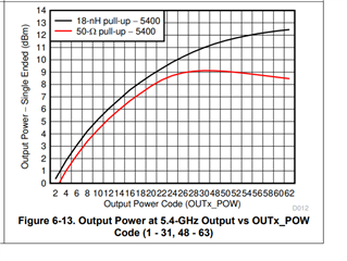
    If we assume 3GHz RFout with a 50Ohm resistor pull up (for good impedance) we can expect about 8dBm of RF power. 

    Output power is adjustable via register config. Also please note you can achieve higher output power utilizing an inductive pull up at the cost of matching. 

    LMX1214 is an RF buffer & divider. Here are the input requirements. 

    As long as your Input swing is within 0 to 10dBM SE, you will not have an issue. 

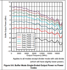
    LMX1214 also has adjustable output power. 

    2. Yes the LMX1214 is a 1:4 buffer thus you can utilize any of the other outputs. 
    According to the ADC DS, the sampling clock specs are as follow: 

    Regards, 

    Vicente