This thread has been locked.

If you have a related question, please click the "Ask a related question" button in the top right corner. The newly created question will be automatically linked to this question.

LMX1214: spi interface

Part Number: LMX1214

Tool/software:

Hi,

We have a customer requirement to interface the LMX1214 clk buff SPI -> opto ISO6721FB -> FPGA

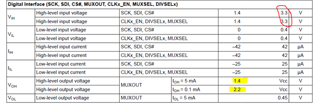
  1. In the LMX datasheet, 2 different values are given for muxout (SPI SDO). Now which VoH value needs to be considered for voltage loading analysis?
  2. shouldn't the ViH max be 2.5V?

Thanks

    1. For voltage loading analysis, consider what loading is closer to your use case. The intent is to demonstrate that at minimal load (0.1mA) MUXOUT can manage VOH voltages close to VCC, but at higher load (5mA) the IR drop across the output PMOS is significant, and can prevent proper 2.5V logic levels from being recognized. Most digital signaling is high-impedance, where the VOH minimum is 2.2V or better.
    2. VIH max is actually is 3.3V. The digital interface pins, when used as inputs, use a Zener clamp to ~3.3V, as opposed to a diode clamp to VCC. This is for compatibility with 3.3V logic levels without needing a level shifter. (A level shifter to a 3.3V controller may still be necessary for MUXOUT when used as SDO pin, if levels above 2.2V are required for logic high signals or if there is substantial loading on the MUXOUT pin anticipated.)
  • Thank you Derek - that helps