Tool/software:
Hi,
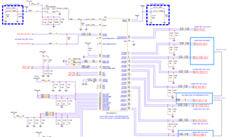
Could you check attached TCS file?
With this tcs, Clock_out0,2 is ok but there is no output at Clock_out1.
Please check what parameter has to be modified.
Fist_LMK04832_config_240905.tcs
Thanks.
Tool/software:
Hi,
Could you check attached TCS file?
With this tcs, Clock_out0,2 is ok but there is no output at Clock_out1.
Please check what parameter has to be modified.
Fist_LMK04832_config_240905.tcs
Thanks.