This thread has been locked.

If you have a related question, please click the "Ask a related question" button in the top right corner. The newly created question will be automatically linked to this question.

LMX1214: SYNC pins

Part Number: LMX1214

Tool/software:

Hi,

We want to interface the FPGA LVDS output to the SYNC pin. Based on below FPGA LVDS output spec, both common mode and differential seem to be out of spec.

 For FPGA outputs from 1V to 1.425V. VCM of SYNC pin starts from 1.2-2V. 

Similarly Vodiff of FPGA is 247 to 454mV. But for CB it starts from 0.6/0.8V

Can you pls suggest how these signals are to be coupled to the FPGA?

  • LMX1214 VCM is the voltage at which the differential inputs are at equilibrium (no current would flow from P to N). Your FPGA LVDS has an approximate VCM of 1.2125V, which satisfies the VCM requirement. The signal amplitude specs are specified as 2 * |Vp - Vm| (not that we mention this anywhere), which means that LVDS with |Vp - Vm| = 425mV is adequate for either DC or AC coupling.

    Typically the VCM/amplitude ranges in the FPGA's LVDS outputs are programmable - do these specs represent a range of possible programmable values, or the actual full range of possible VCM/amplitude for the nominal LVDS output? If it's the former, there's no issues. If it's the latter, you should probably AC-couple the LVDS instead.

    The LMX1214 datasheet tremendously botches the recommended operating conditions for the SYNC input, so I'll try to explain the operating theory:

    • The absolute DC voltage value at the pins should not be below 0.8V during normal operation, as this is outside of the compliance of the internal input amplifier's current source. DC voltage < 0.8V is fine at startup, or if input is unused and left floating/driven by tri-state - it doesn't cause damage to the device, just saturates the input amplifier or turns off that leg of the differential pair, preventing the amplifier from generating high-slewrate edges needed to align the SYNC with a specific CLKIN clock cycle at higher frequencies. I'm unsure what happens if the pins are driven below 0.8V with a low-impedance source, but there's nothing in the absolute maximum ratings about this, so I assume it's not a cause for concern electrically, just functionally.
    • The magnitude of the differential input signal directly determines what common mode level is acceptable. For a signal that swings ±200mV from a common mode voltage (e.g. LVDS), anything that satisfies the condition of > 0.8V during normal operation is acceptable, so the minimum acceptable common mode is actually 1.0V in this case. For a signal that swings ±400mV from a common mode voltage (e.g. LVPECL), 1.2V is the minimum acceptable common mode voltage.
    • The AC-coupled and DC-coupled signal magnitude in the datasheet are slightly different because of the presumed possible common mode biases produced by the LMX1214 for AC-coupled scenarios. I suspect not much thought was put into how best to represent these conditions. A better description of these ratings would show the limits according to the corresponding bias settings for the SYNC input.
    • There's not a lot of hysteresis on the inputs, and from our testing we observed that the SYNC pins can oscillate if left undriven, or if AC-coupled without following the recommended structure in datasheet Figure 8-2 or 8-3. The AC-coupling amplitude limits are specified in consideration for the limited hysteresis, and the actual magnitude of signal required to overcome the bias caused by the pull-up and pull-down resistor biasing in a typical AC-coupled configuration. In the DC-coupled case, I've had no trouble driving the input with ≥100mV difference between the pin voltages, so I'm not sure what reasoning (if any) is behind specifying DC-coupled minimum amplitude at 0.6Vpp. 1mA across the internal 100Ω termination is more than enough to eliminate oscillation concerns.

    I will endeavor to get these clarifications inserted somewhere in the LMX1214 datasheet - it is very frustrating to read conventions assumed without explanation, values pulled essentially out of thin air, and non-obvious LVDS compatibility out of what's there.

  • Hi Derek,

    Thank you for taking your time to provide the insights.

    The LVDS limits specified in the FPGA datasheet are complete range and not programmable.

    With that, can you pls confirm if my below summary of your explanation is correct?

    1. Even though FPGA LVDS output will be 1V to 1.425V (with no option to tune), since the Clkbuffer can read 1V-2V, common mode voltage compatibility can be achieved. 

    2. Even though FPGA LVDS output swing will be 247-454mV, the clock buffer can read it since it's input differential voltage capability is from 200mV to ~600mV. Hence differential mode voltage compatibility is also achieved.

    3. Based on points 1 & 2, we can go with DC-coupling termination as suggested in figure7-4

    Thanks

  • With the knowledge that this is not programmable, we do have a corner where there may be cause for concern: suppose the common mode voltage is 1V, and Vodiff is 600mV. In that case, we'd have 0.7V actively driven on one of the inputs at steady state for any DC-coupling. This could impact the slew rate of the SYNC input amplifier, which could affect timing stability.

    If this corner is possible on your FPGA, you should AC-couple the signal instead as per Figure 8-2 in the datasheet. I recommend setting the internal bias to none (as though DC-coupled) and using external resistors to set the bias. While the datasheet recommends having at least 150mV potential across SYNC_P and SYNC_N, as stated before I've seen this work with 100mV. With R2 = R3 = 1kΩ you'll have about 120mV, which approximately splits the difference in the worst case when the FPGA output is only 250mV swing so that both logic high and logic low conditions see ±125mV at their respective pins. Likewise, for pulsed inputs up to 450mV, the SYNC_N pin will be brought no lower than 0.9V from steady-state.

    With this scheme, there could be a momentary condition where SYNC_P drops below 0.8V if the input amplitude is 450mV, the input is logic-HIGH, and the AC-coupling network has settled such that SYNC_P starts at 1.13V - a 450mV input pulse could temporarily pull SYNC_P voltage down to 0.68V - so I recommend pulsing the SYNC input to avoid this condition, or else ensuring that the SYNC subsystem in the LMX1214 is not enabled when restoring SYNC input to logic-LOW and allowing adequate time for the input to return to nominal biasing.

    On the other hand, if the FPGA's VCM and Vodiff are linearly correlated such that the 250mV swing occurs at 1V VCM and the 450mV occurs at 1.425V VCM, with a continuous proportional relationship between VCM and Vodiff, direct DC-coupling would satisfy all requirements. I doubt that the VCM/Vodiff are linearly correlated like this, but I mention it just in case, as it would simplify the story.

  • Hi Derek,

    • I don't think it's safe to assume linear correlation between VCM and Vodiff in FPGA's side.
    • We are thinking of driving a 0 to 1 (low to high) pulse on SYNC_P/N from FPGA and maintaining it '1' (HIGH) always until a system-level reboot happens. 
      (a) Is that sufficient for the sync signal to work as desirable?
      (b) If yes, Is it safe to keep options for both AC and DC coupling discretes on the board and populate the AC coupling network as default in BOM just to be safe? or would you recommend keeping only one? and which one would that be? 

    Thanks

  • Hello Derek,

    Can you please respond on this?

    Thanks

    Nandini

  • Apologies for the delay...

    a) Yes, holding the SYNC at logic HIGH for the remainder of operation should still work with AC-coupling. There will be a momentary condition when system-level reboot happens where the SYNC signal returns to logic LOW from the FPGA, and the absolute value of the pin voltage drops below 0.8V, during which you should wait for the pin voltages to return to the default biasing for the AC-coupling - you can estimate how long this takes with a straightforward SPICE simulation (assume the SYNC_P to SYNC_N path within the LMX1214 is a 100Ω resistor, this is close enough for timing estimates), and you should be able to reduce the waiting duration (and the resulting pulse width at the SYNC_P/SYNC_N pins) by reducing the size of the AC-coupling capacitors.

    b) You can keep both AC- and DC-coupling options on the board, and the recommended circuit in the datasheet suggests an external passive network that should allow for switching between AC- and DC-coupling options as needed.

  • Thank you, Derek - this helps.

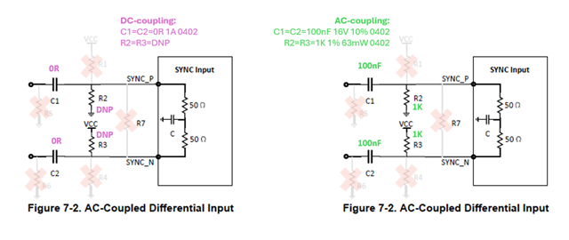
    Are these terminations ok to give option for both DC and AC-coupling?
    Pink DC coupling and Green are for AC coupling.

    Since we plan to use differential LVDS from FPGA - R1, R2, R5, R6 are not needed and R7 is not needed since 100-ohm internal termination is available in clock buffer. 

    Is my understanding correct?

    (We will check the time delay in simulation for 1nF per below circuit.)

    Thanks

    Nandini

  • Your circuit, and the proposed components for DC- and AC-coupling, are correct.

  • Thank you Derek for your timely support.