Other Parts Discussed in Thread: AFE7950, AFE7950EVM
Tool/software:
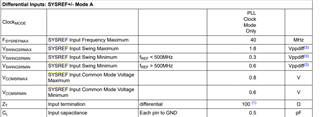
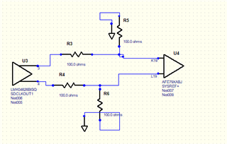
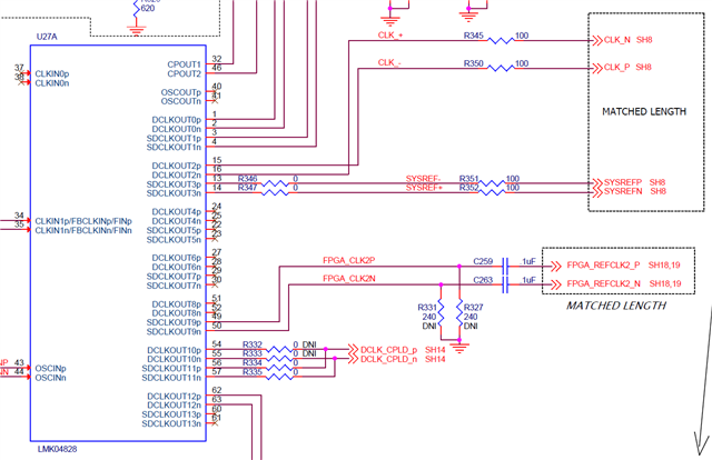
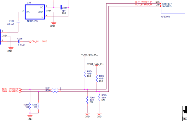
I am looking at the AFE7950EVM reference design and there is a SDCLKOUT3 differential clocking signal going from the LMK04828 to the AFE7950. The signals run through a series 100 ohm resistor and then a 100 ohm resistor to ground before reaching the differential 100 ohms on the AFE7950 SYSREF input.
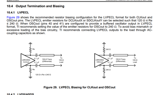
Presumably this termination scheme is meant to keep the output of the LMK04828 within the allowable voltage range of the AFE7950.
Given the format options for the SDCLK output and the termination chosen the output is likely LVPECL.
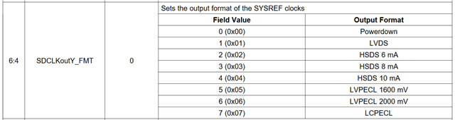
Is my assumption about the output format correct? If it is, how can one calculate the common mode voltage at the output of the driver? The termination resistors are spread across the clocking and transceiver schematic pages. Where should they be placed in the layout relative to the driver and receiver chips?