LMK00301: Application consulting

Part Number: LMK00301
Other Parts Discussed in Thread: LMK1D2102

Tool/software:

Dear Experts,

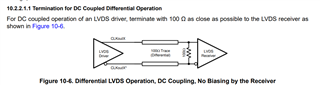
We are selecting a clock buffer that meets the requirements of one 27MHz differential clock input (LVDS) and two 27MHz differential clock outputs (LVDS). We are currently evaluating LMK00301 and are unsure if the chip can meet the requirements. There are some questions that need to be answered by experts
1. Can LMK00301 support our 27MHz clock frequency application scenario?
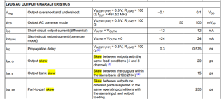
2. Does the SKEW standard also apply to differential output at 27 MHz?
3. Can channels and external clock input pins that are not used by the chip be NC when not in use?
Looking forward to your reply. Thank you very much

  • Hello Chen, 
    We have dedicated LVDS buffers. 
    LMK1D2102 family can better meet your needs and its newer part. 

    LMK1D210x Low Additive Jitter LVDS Buffer datasheet (Rev. B)

    The 27MHz input is supported. 


    I am unsure of what you mean by the skew standard - can you please elaborate? 
    Are you asking about output-to-output & p2p skew? 

    Unused inputs and outputs can be left floating for LMK1D210x as well. 

    Best regards, 

    Vicente

  • Dear Vicente,

    Thank you for your response and recommendation. After project evaluation and planning, we have selected LMK00301. We still have some design questions about LMK00301 and hope to receive your answers
    1. The specification sheet does not specify whether LMK00301 comes with a 100 Ω internal termination, and how to design the external matching circuit for LVDS signal input


    2. If 100 Ω is added in front of the AC capacitor, then a bias of 50 Ω is applied behind the AC capacitor. According to the data manual description, for LVDS drivers, will it become 50 Ω and can the differential level still exceed 250mV?

    3.The following is the CDCLVD1204RGTR block diagram we previously applied. Currently, we need to modify block diagram B to LMK00301. How do we need to make the changes and what are the points to note

    I hope to receive your response. Thank you very much

  • Hi Chen,

    Vicente is out of office today. Expect to hear back by the end of the week.

    Thanks,

    Michael

  • Hello Chen, 
    1. LMK00301 input does not have intenal 100Ohm differential termination on CLKinx
    If utilizing a LVDS input to LMK00301 use DC coupling as it's the easiest to implement. Use the following termination scheme. 


    2. This is assuming that receiver has internal biasing. 
    If that's the case - you will need to AC couple the LMK00301 input to avoid damaging the receiver input. 
    If your receiver does not have internal biasing - than this is not a cause for concern.  

    3. If the driver is an LVDS signal - I recommend DC coupling and just having the 100Ohm differential termination near the pin.
    in other words, follow the termination scheme I attached in answer 1 where the LVDS receiver is the LMK00301 input. 
    Best regards, 

    Vicente 

  • Hi Vicente 

    You mean LMK00301 does not have an internal bias voltage? If we want to do AC coupling, how to add the external bias voltage and what level ? Thank you

  • Hi Chen,

    if the driver is LVDS it should have an a common mode voltage. 
    if we don’t AC couple - we don’t need external biasing.

    best regards,

    Vicente 

  • Hi Vicente,

    Sorry, maybe I didn't make myself clear. Our driver is LVDS and the receiver is LMK00301. If we use AC coupling connection, how can we add external bias? Thank you

  • Hi Chen, 
    If the driver is already LVDS - why do you want to AC couple? There is no incentive to AC couple if the driver is already LVDS. 

    If the driver is LVDS - DC couple the LMK00301 inputs and will just need the 100Ohm differential termination. 

    Best regards, 

    Vicente