Part Number: LMK04208
Tool/software:
Hi,
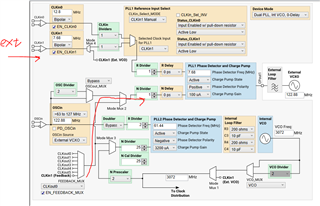
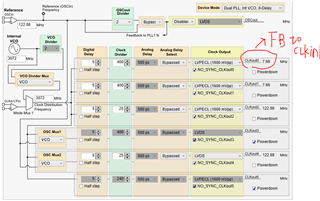
I want LMK04208 work at Dual PLL, Int VCO, 0-delay mode on my board. It will feedback CLKout0 to PLL1 in the internal path as below figure shown. Clock setup is listed below:
CLKin1: external 7.68MHz sine clock from signal generator
CLKout0: 7.68MHz
CLKout1: 7.68MHz
CLKout2: 122.88MHz
CLKout4: 122.88MHz
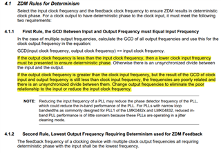
Test with oscilloscope, I find that CLKout0 and CLKout1 couldn't be aligned, and also don' t have fixed phase relation over power cycle. I think this clock plan or setup conform to two rule of Zero-delay mode totally. But CLKout1 couldn't share the same phase relation with CLKout0 against CLKin1, why?
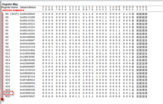
attach the .tcs file for your inspection.
122M88_PL_122M88_SYSREF_7M68_clk5_12M8_MCS_No_Sync_V4.tcs


Thanks in advance!
Best regards!
Jason


