This thread has been locked.

If you have a related question, please click the "Ask a related question" button in the top right corner. The newly created question will be automatically linked to this question.

LMK04832: Inquiries regarding PLL settings.

Part Number: LMK04832
Other Parts Discussed in Thread: LMX2594, LMX2820

Tool/software:

Hi ALL,

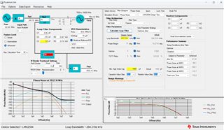
I would like to make a continuous clock with a square wave for the 1.92MHz Clock OUTPUT using the LXK04832 PLL IC, but a pulse-shaped waveform is being output as shown in the attached photo.

Please help me as to why it is output like this. Attached is the XX.TCS file

Thanks.

Second_LMK04832_config_240924.tcs

  • Hi ALL

    I have one additional question from the above. I am curious why Clock Output1 (1.92MHz) is measured at 3.36Mhz. 
    1.92MHz must be measured. Please check the TICS program.

    Thanks.
  • Hi Kyu, 
    Are both PLLs locked? 
    You can set PLLx_LD_TYPE to PLLx DLD and it should be high for each respective PLL if locked. 

    Are you using your own custom board or the EVM? 

    If you're using the EVM - ensure you have the correct termination on the output for LVDS. The EVM by default has different outputs configured for different output formats. 

    On a side note - why not use a 122.88MHz VCXO instead of 100MHz? 
    This will increase the PFD of PLL2 and reduce the N divider value which will result in better PN performance. You can utilize a 2949.12MHz VCO frequency instead of 2457.6MHz to generate the outputs you need. 

    Best regards, 

    Vicente 

  • Hi  Vicente

    Both PLLs are locked. There is no evm board, and a self-developed board is being tested.
    What I/O do you recommend setting the PLLx_LD you mentioned? Also, what improvements will be made if you set it this way?

    Thanks,
    KB
  • Hi KB, 

    The PLLx_LD settings are available only for PLLx_LD_Type which are outputted to the status_LD pin on the IC. 

    Can I receive a copy of your schematic? 

    Also given you require a 2457.6MHz VCO frequency - instead of 100MHz VCXO can you utilize a 122.88MHz VCXO? Your PFD for PLL2 will be much larger and thus your N divider will be reduced for better PN performance. 

    Besides this I don't see anything wrong with your configuration - everything looks okay. 

    If you switch output formats or check different outputs - do you encounter the same issue? 

    Best regards, 

    Vicente 

  • Hi Vicente

    I will test the VCXO you recommended at 122.88MHz and let you know the results.

    Attached is the schematic for the LMX2594.

    Regards

    KB

  • Hi KB, 
    Are you having trouble with LMX2594 as well? 

    What is the reason for the 10k PD resistors on SYNC & SYSREFREQ?

    You can also connect the LMK differential outputs to the SYNC or SYSREFREQ signals directly. 

    Did you design loop filter on PLLatinumSim? 

    Also - are you still having issues with LMK04832? 
    Best regards, 

    Vicente 

  • Hi Vicente

    Additionally, I am attaching the LMK04832 schematic.
    The pull-down resistor on the SYNC/SYSREFREQ pin of the LMX2594 is currently in DNI (Do Not Install) status.
    Also, as you mentioned, I used the PLLatinumSim tool to calculate and apply the loop filter values in the design.

    Could you please review the loop filter calculations in the attached xx.tcs file to confirm they are correct?

    Regards.

    KB

  • Hi Vicente

    Regarding the VCXO change, here are the simulation results for xx.TCS and xx.sim after changing to 122.88MHz.
    Please check to ensure the calculations are accurate.

    1. LMK04832

      - OSC_IN : 122.88MHz

      - CLKin0 : 245.76MHz 

    2. LMX2594

      - OSC_IN : 122.88MHz

      - RFOUT A : 3.932.16MHz

      - RFOUT B : 1.92MHz

    Regards,

    KB

    PLL2_LMK04832_122.88-1031-t.tcsPLL3_LMX2594_122.88-1031-t.tcs

  • Hi Ryu, 
    For the LMK04832 it looks good. 
    My question is for LMX2820 - do you really need the 36kHz loop bandwidth? 

    I see in the PLLatinumSim config you have it calculated for that bandwidth. 
    Nevertheless, I would also use the input doubled in the LMX2820 input path instead of the divider which will also reduce your N divider value for better PN performance. I also saw a bunch of red so I want to assume this was configured incorrectly as the PFD_SEL option was disabled and the Pre-R Post-R, MULT, N divider and VCO value were incorrect. 
    Please try this instead. 


    Best regards, 

    Vicente 

  • Hi Vicente

    The part we are using is the LMX2594. The 36kHz BW was automatically calculated in SIM TOOLS.

    Is there an issue with the 36kHz BW? Please refer to the image below.

    We need your assistance with the LMX2594 loop filter values. Could you please send us the simulation results R,C ?

    Also, the tool shown below is different from the tool GUI we have. Is this a new version release?

    As you mentioned, when we set the doubler to x2, the N divider turns red, and the RFOUT does not display the desired value.

    Could you simulate this part as well and provide the results?

    Please refer to the image below.

    Regards,

    KB

  • Hi Vicente

    Here is a simulation image of the LMX2594's LOOP Filter values using the PLLatinum tool. Please review it.

    Regards

    KB

  • Hi Kyu, 
    Sorry for some reason I loaded 2820 - my apologies. 
    I would recommend the following configuration if possible. 
      

    Your loop filter is stable in this scenario. 

    In reality I cannot tell you how to design your loop filter as the loop bandwidth requirement is dependent on your application. 

    For example, some customers need the fastest lock times possible and thus make the loop bandwidth as large as possible. 
    Other customers require extremely narrow loop bandwidths. 

    I would go with the result below: 

    But like I mentioned my approach is to always make the PFD as large as possible which reduces the N divider values which results in better PN performance.


    If your application requires a 54kHz loop bandwidth - the loop filter is stable, but I would first use the doubler. 
    Using the doubler and designing for a 54kHz loop bandwidth would be as follows: 

    Also - please ignore the red. 
    In TICSpro if we reduce the MASH order, we can have N divider smaller than 36.

    Best regards, 

    Vicente

  • Hi Vicente

    We have confirmed the RFoutA 3932.16MHz output as normal using a 122.88MHz input source. However, RFoutB REF-CLK 1.92MHz is still an issue.

    We have a request regarding the verification of the RFoutB SYSREF CLK 1.92MHz output.

    Could you provide us with the actual waveform measurements for RFoutA at 3932.16MHz and RFoutB at 1.92MHz using the EVM board you have?

    The image below shows the complete PLL Clock block diagram of our board.

    We kindly ask you to refer to it and confirm the desired clock through simulation and send us the results.

    A lot of time has already been delayed, so we would appreciate your prompt response.

    Regards,

    KB

  • Hi KB, 
    I think I see your issue. 
    When utilizing SYSREF output for LMX2594 it requires the VCO_PHASE_SYNC bit to be set. 
    Enabling this bit changes the IncludedDivide value from 1 to 4 given our output divider needs to be set to 2 to generate 3932.16MHz
    This also reduces the overall N divider value (now reduced to 7) to a number no MASH order can support as the minimum N divider value must be 28 for any modulator.


    Unfortunately LMX2594 will not be capable of generating the 1.92MHz output. 

    Best regards, 

    Vicente 

  • Hi Vicente,

    I understand the content well. Then, is there any issue with the 1.92 MHz in the LMK04832?

    Is it possible to measure whether the clocks in the PLL Tree configuration we provided (245.76 MHz, 61.44 MHz, 1.92 MHz, etc.) are functioning correctly on the LMK04832 EVM board?

    If the operation is confirmed, please also send it in the xx.tcs file.

    Let me know if this works for you!

    Regards,

    KB

  • Hey Kyu, 
    I went into the lab and tested this. 
    I managed to get the LMX2594 to lock and got the 1.92MHz SYSREFOUT. 

    1.92MHz SYSREFOUT.tcs

    I just connected to scope SE without terminating unused end but nevertheless just wanted to prove it functions, the device locks & the outputs are correct. 

    Best regards, 

    Vicente 

  • Hi Vicente

    I have confirmed that the LMX2594.TCS file you sent works well at 1.92M & 3.392.16MHz.
    However, the 1.92M output is still not functioning on the LMK04832.
    Could you please test it on your EVM board, as you did with the LMX2594, and let us know the results?
    Thank you for your continuous support.

    Regards,

    KB

    4o
  • Hello Kyu,
    I have checked this on bench.

    Try this config.

    Best Regards, 

    Vicente 
    LMK04832_245.76MHzCLKIN1_122.88MHZOSCIN_2949.12MHZVCO.tcs


  • Hi  Vicente

    I have a question regarding the LMK04832.
    The input Fosc is 10MHz, Fpd is 0.4MHz, Fvco is 2457.6MHz, and Fout is 245.76MHz.
    When measuring the output frequency and the reference frequency simultaneously with an oscilloscope, the output frequency should remain synchronized to the reference clock of 10MHz. However, the synchronization is not maintained, and the output frequency does not stay stable at the reference point but fluctuates.
    Attached is the xxx.tcs file and a PLLatinum capture image for your reference.
    I would appreciate your advice.

    Regards,

    KB

    LMK04832_PLL1_20241116.tcs

  • Hi Kyu,

    Do you no longer want to use 122.88MHz? 
    The loop bandwidth of this device is extremely narrow - are you trying to jitter clean? 

    If you monitor lock detect does the pin stay high or does device lose lock? 

    Best regards, 

    Vicente

  • Hi Vicente

    Our board is designed to use an external input clock operating at 10MHz.
    As per your instructions, we performed jitter cleaning and recalculated the loop filter values.
    Please refer to the attached capture for details.
    Additionally, the lock detect pin is high.

    However, the input and output clocks are still not stable.
    Could you urgently check where the issue might be?

    Your prompt response would be greatly appreciated.

    Best Regards.

    KB

  • Hi Kyu, 
    You originally stated this. 

    CLKinX was 245.76MHz - this is valid as the R divider will be 2 * N divider thus fOSC being 122.88MHz which will result in a lock. 

    If you're jitter cleaning, yes this is accomplished utilizing PLL1 with a very narrow loop bandwidth to allow for the VCXO noise to dominate. 
    But you need to have a CLKINx frequency that can drive the 122.88MHz external VCXO with an integer relationship. 
    There is no way to drive an external 122.88MHz VCXO from a 10MHz input. 

    The following mathematical relationship must be met where fVCO = 122.88MHz & fOSC = 10MHz with both N & R being integer values. 
    I find it extremely hard to believe you have achieved lock in PLL1. 

    The 122.88MHz external VCXO which is driven by PLL1 gets fed into OSCIN for CLK distribution - the PFD of PLL2 is 2457.6MHz. 

     You can input a 10MHz input to OSCIN directly to generate the 2457.6MHz VCO frequency by operating LMK04832 in single loop mode but you will no longer be jitter cleaning and your output phase noise will suffer a bit - as you can see in the PLLatinumSim screenshot you shared where the Fpd frequency is very low and the N divider is very large (6144). 

    If you want to jitter clean using PLL1 to drive an external 122.88MHz VCXO you need to ensure fOSC is a value that meets the integer relationship from the equation i sent above. 

    You cannot accomplish this using 10MHz. 

    Best regards, 

    Vicnete 

  • Hi Vicente

    The PLL mentioned above (245.76MHz input) refers to PLL-1 in the Clock Tree image I shared previously.

    Overall, I understand the points you have made.
    Am I correct in understanding your conclusion that to synchronize the clock with a 10MHz input, an additional 122.88MHz oscillator is required?

    I plan to revise the circuit as shown below. Please confirm.

    Best regards

    KB

  • Hello Kyu, 
    I have found a R & N divider that meets your 10MHz CLKin requirement to drive a 122.88MHz external VCXO. 

    A 0.08MHz PFD will work. This will drive your external VCXO accordingly and you will be able to jitter clean with a small loop bandwidth. 

    Best regards, 

    Vicente 

  • Hi Vicente

    Please confirm whether the PLL R&N Divider you found meets the following conditions:

    1. Input Reference Clock: 10 MHz
    2. External OSCin: 122.88 MHz
    3. Output: 61.44 MHz, 245.76 MHz, etc.

    If the above conditions are correct, does this mean that these conditions can only be satisfied in dual-loop mode, and not in single-loop mode?

    Is there any way to meet the following conditions in single-loop mode?

    1. Input Reference Clock: 10 MHz
    2. Output: 61.44 MHz, 245.76 MHz

    I deeply appreciate your advice.

    Best regards

    KB

  • Hi Kyu,

    Please find the attached images of the single-loop setup with your specifications. Please note that using this configuration, as opposed to the what Vicente suggested, will result in a poorer phase noise performance - if you have a clean input source, then this will be fine, but if you do not, I would suggest the dual loop configuration proposed above. 

    Thanks,

    Michael