Tool/software:
The datasheet for the LMX2486 indicates that a 39Ω resistor and a 27pF capacitor should be placed in front of the High Frequency Input Pins.
Do this resistor and capacitor affect the bandwidth and phase margin of the loop filter?

This thread has been locked.
If you have a related question, please click the "Ask a related question" button in the top right corner. The newly created question will be automatically linked to this question.
Tool/software:
The datasheet for the LMX2486 indicates that a 39Ω resistor and a 27pF capacitor should be placed in front of the High Frequency Input Pins.
Do this resistor and capacitor affect the bandwidth and phase margin of the loop filter?

Hi Noel Fung,
Thanks for the answer!
Is the phase of the feedback signal delayed by the resistor or capacitor?
I think that if the phase delay is too large, the PLL will not operate normally and the feedback will not function.
Hi Watanabe-san,
Yes, maybe there will be a small delay due to the R and C and the distance, but this delay is not matter.
Hi Noel Fung,
Thank you for your reply. I have understood the content.
In addition, I would like to ask the following items below.
・Does the phase delay increase as R10 is increased?
・Is the input signal strength of the FinRF pin determined by the voltage divider ratio between the surrounding R and C and the input impedance of the IC?
If the signal strength falls below the Input sensitivity of the FinRF pin (-10 to 0 dBm for the LMX2486), will the output frequency from the VCO be uncontrollable?

Hi Watanabe-san,
R8, R9 and R10 forms a T-power splitter. C9 is simply a DC-block. There is nothing wrong with these components.
If it is unlock, either the loop filter is not stable, the feedback signal is too small, OSCin signal is too small or programming is not correct.
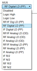
use the MUX to debug. For example, if you set MUX to RF R/2, you should get a signal at FTEST/LD pin with frequency = 1/2 phase detector frequency. If you don't see anything, either OSCin signal is too small or programming is not correct. To verify programming, set MUX to Logic High, FTEST/LD should be HIGH.

Hi Noel Fung,
We are currently designing a circuit to variable the power of the VCO output signal by connecting PIN diodes.
When the power is large, we can control the frequency. When the power is small, we can’t control it. Therefore, I believe there is no issue with the oscin or program settings.
I think the problem might be caused by a feedback signal that is too small.
If so, what should we do to control the power as small as possible ?
Watanabe-san,
Noel is currently out of office, please expect a response by tomorrow.
Thanks,
Kadeem
Hi Watanabe-san,
What is the output power at RFout (after R9)? This is also the power input to RFIN pin. Datasheet requests a min. of -15dBm.
You can use MUX to verify RFIN signal. Set MUX to RF N/2, check FTEST/LD pin, you should get a signal with frequency = VCO/N/2.
Hi Noel Fung,
I apologize for this late reply.
This is a different circuit from the typical application, but when R10 (feedback resistor) is 300Ω, the RF output power can be adjusted from -5dBm to -12dBm. (If it goes below -12dBm, the frequency cannot be controlled.)
However, when R10 is 39Ω, the RF output power can be adjusted from -7dBm to -25dBm. (If it goes below -25dBm, the frequency cannot be controlled.)
Why does changing the resistance value of R10 allow control of smaller power?
I checked the FTEST/LD pin. When the power decreases and the frequency cannot be controlled, the VCO/N/2 signal cannot be obtained.
Hi Watanabe-san,
I don't understand, how can we adjust the output power? Do you have a schematic?