This thread has been locked.

If you have a related question, please click the "Ask a related question" button in the top right corner. The newly created question will be automatically linked to this question.

LMK00334: Selection of Common clock from SOM or SRNS with a local clock.

Part Number: LMK00334
Other Parts Discussed in Thread: LMK00101

Tool/software:

Hi,


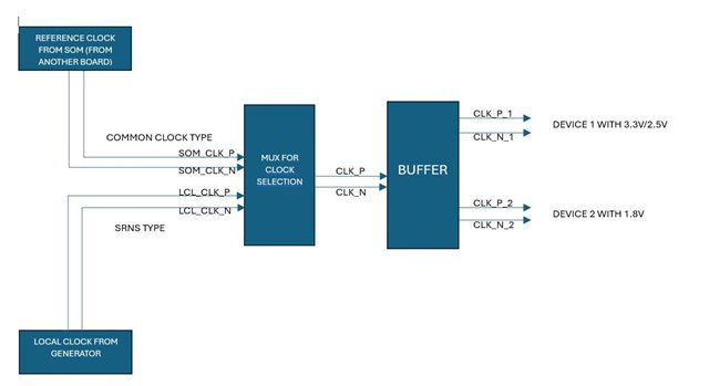
 I have this requirement, a reference clock for PCIe Gen 3 is coming from SOM module to our PBA, at the same time I need to local clock available in my PBA so I can select. Here question is can I use LMK00334 for this application? and the other question is can I use the clock out of this to a device which operates at 1.8V? 

  • Hi Adarsh,

    I just want to make sure that I understand what you need. Do you need a clock buffer that can simultaneously output a 3.3 V/2.5 V signal and a 1.8 V signal? Or do you need one that allows for input clock selection, that will then output either the 3.3 V/2.5 V signal or the 1.8 V signal? Additionally, what will be the frequency of the input signals that the buffer will need to support?

    Thanks,

    Michael

  • Hi Adarsh, 
    Yes, LMK00334 is suitable for this application. 
    VCCOx only operates at 2.5V or 3.3V though. 


    Best regards, 

    Vicente 

  • Hi Michael,

    Here the interested signal frequency is 100MHz,

    My requirement is (Same captured in block diagram), 100MHz of reference clock will come from SOM to My PBA. My PBA has MUX in first stage which selects clock either from SOM or local clock which is also 100MHz (generated by a clock generator in My PBA), it is kind of selecting common clock or SRNS clock. Once the required clock is selected by MUX i.e either from SOM or local clock, the next stage will be a buffer which takes one input and the output of the buffer would be 2 nos, one with 3.3V/2.5V out and the other one is 1.8V out of same frequency i.e 100MHz. 

    Since LMK00334 has MUX in first stage which can select either of 3 inputs and the output goes to a buffer which has 2 banks each bank having 2 pairs, I thought I can use this device? Bank A for 3.3V/2.5V PCIe reference clock and the other Bank B 1.8V PCIe reference clock?

  • Hi Vicente,

    If that is the case since the output is HCSL (3.3V for example), can this HCSL output be used for a device which is operating at 1.8V?

  • Hi Adarsh,

    The LMK00334 is not capable of providing your specifications. It cannot output a signal with less than 2.5 V of amplitude. The LMK00101 satisfies your specifications (LMK00101 data sheet, product information and support | TI.com). It is a universal buffer, and it offers two output banks that can simultaneously output 2.5/3.3 V and 1.8 V signals. 

    Thanks,

    Michael

  • Hi Michael,

                      I was referring to the forum discussions and datasheet spec captured below.

    e2e.ti.com/support/clock-timing-group/clock-and-timing/f/clock-timing-forum/584859/lmk00334-output-voltage-levels

    e2e.ti.com/support/clock-timing-group/clock-and-timing/f/clock-timing-forum/823335/lmk00334-q1-can-clock-buffer-output-and-input-in-same-voltage-level

    Hence was my question how VCCO supply would impact the HCSL output when my receiving end is operating at 1.8V (PCIe Switch).

  • Hi Adarsh,

    I understand your question now. HCSL is a current-based driver, which means that you can adjust the swing with a voltage divider (series resistor followed by shunt resistor) without having to change anything else about the system. If you want a 1.8 V signal from a 3.3 V output, you would need to instantiate a series resistor with a value that is equal to 5/6 of the shunt resistor (i.e. 150 Ohm series and 180 Ohm shunt). 

    Thanks,

    Michael