Part Number: LMX2582
Tool/software:
HI ,
In our Design, LMX2582 PLL is used and programmed by FPGA using SPI interface. We have used TICS PRO Software and generated an HEX File
Below are the queries:
- What should be the sequence of programming ?
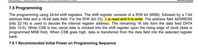
Is it from R0,R1,...R70 OR R70,R69,...R0? - In registers R68,R69,R70 in datasheet MSB is given as Read (1) but in HEX File for these three registers MSB is (0) ? Kindly clarify.
- What is the PLL Lock register number ?
- Are there any other registers you would recommend for FPGA to poll/read during/after PLL SPI configuration?
I have attached Both TICS file, HEX File , Datasheet Images FYR. Kindly check and respond
TI_PLL_TICS_20241112_Powerset.tcs
R70	0x460000
R69	0x450000
R68	0x440089
R64	0x400077
R62	0x3E0000
R61	0x3D0001
R59	0x3B0000
R48	0x3003FC
R47	0x2F00CF
R46	0x2E0720
R45	0x2D0000
R44	0x2C0000
R43	0x2B0000
R42	0x2A0000
R41	0x2903E8
R40	0x280000
R39	0x278104
R38	0x260036
R37	0x254000
R36	0x240C11
R35	0x23021F
R34	0x22C3EA
R33	0x212A0A
R32	0x20210A
R31	0x1F0601
R30	0x1E0034
R29	0x1D0084
R28	0x1C2924
R25	0x190000
R24	0x180509
R23	0x178842
R22	0x162300
R20	0x14012C
R19	0x130965
R14	0x0E0FFC
R13	0x0D4000
R12	0x0C7001
R11	0x0B0018
R10	0x0A10D8
R9	0x090302
R8	0x081084
R7	0x0728B2
R4	0x041943
R2	0x020500
R1	0x010808
R0	0x00221C