Because of the Thanksgiving holiday in the U.S., TI E2E™ design support forum responses may be delayed from November 25 through December 2. Thank you for your patience.

LMK04828: KVCO and VCOCap values in PLLatinum Sim for LMK04828B when used with external VCXO

Part Number: LMK04828

Tool/software:

Hello,

I have query regarding the PLLatinum simulation.

We are using LMK04828B with external VCXO option in the PLLatinum simulation and have come up with following values for both PLL1 and PLL2 and used the same the filter values connected at CPout1 and CPout2 as shown below.

But regarding PLL1 specifically, when I am loading the device with external VCXO, PLLatinum Sim loads with KVCO and VCOCap values as shown below (Charge pump current (Kpd), input and output frequencies are what we are using in our design currently so are correct).
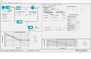
Default KVCO value is 0.0025 MHz/V when loading up the PLLatinum Sim as above.

Default VCOCap value is 0pF when loading up the PLLatinum Sim as above.

But as we are using an external VCXO of which datasheet link I have mentioned it below:

CVHD-950

After looking into an external VCXO datasheet I have changed both VCO characteristics values (KVCO and VCOcap) as shown below.

I have converted 25ppm tuning sensitivity to Hz (from VCXO datasheet) and used that value in KVCO field and I thought VCOCap would be the output capacitance and used 15pF from the VCXO datasheet and placed it in VCOCap field below.

After using these values we have different loop filer 2nd order values to the one from default values and these values we have used in our design.

I have now following queries,

1. Do we just leave both KVCO and VCOCap values as it is when PLLatinum Sim first load up after selecting LMK04828 w/external VCXO?

2. How would we can get the VCOCap value?

3. What I have done to find the loop filter values by changing the KVCO and VCOCap values as shown in second screenshot is right or wrong? and what could I do to make it right?

Thanks,

  • You definitely have to set Kvco and VCOCap yourself, as this does affect the loop filter behavior - maybe for this case VCOCap isn't that important, but definitely Kvco is directly proportional to loop gain and must be configured properly.

    If we have a 76.8MHz VCXO, with 25ppm/V tuning sensitivity and 3.3V of adjustment range, this works out to 76.8MHz * 25ppm/V = 0.00192MHz/V, which appears to be the value you computed as well.

    15pF is listed under output specs, and is thus a representation of the maximum load the output can drive, not the capacitive load presented by the tuning port. If the manufacturer doesn't provide a good estimate of the tuning port voltage, it's reasonable to assume a few pF at most, usually on the low end. Since this is in parallel with C1, typically the effect of just leaving it at 0pF is minimal, and if you observe noticeable differences on-board, you can substitute the value of C1 for a slightly smaller capacitor to compensate; however, for low loop-bandwidth PLLs like this, the usual game is to design the loop filter such that C1 is large enough to render the VCOCap value insignificant by comparison.

    There's a poorly-documented option in PLLatinum Sim 1.6.7, under the "options" menu, labeled "Main Diagram Updates Performance Metrics" that needs to be disabled to prevent changes to Fpd and other settings from reverting the Kvco and VCOCap values to the defaults. The reason this default behavior exists is for devices with integrated VCOs, as the Kvco and VCOCap values may change depending on VCO core and frequency. I have asked, frequently, for this behavior to not be the default when external VCOs are used, but for now there's no mechanism in PLLatinum Sim to distinguish between an integrated VCO and a non-integrated VCO, so we have to do it this way. In other words, it's bewildering, but at least possible, to substitute your own values for VCO characteristics and have them stick through main diagram changes.

    A few other comments:

    • On the Phase Noise tab, in the upper left, under "Graph Settings", you can disable "autoscale axes" and set the x-axis minimum to 1Hz or 10Hz for a better representation of the close-in behavior. PLLatinum Sim was originally designed for our RF PLL product line, so the default axis scaling isn't the best choice for low-bandwidth loop filters.
    • The low Kpd and Gamma values, as well as the very high phase margin, are reducing the component values by a lot, which results in a loop filter that's mostly dominated by the PLL and filter component noise contributions. You could try something like Kpd = 0.35mA, phase margin = 60°, Gamma = 1, and still get something that's plenty stable, but gives back a lot more performance at the 1kHz offset and above.
  • Hi Derek, 

    thankyou for the reply and explaining in detail. This reply has solved our query regarding PLLatinum Sim and also thanks for sharing good tips at the end.

    I do have separate query related to VCC1_VCO.

    We have 4 batch of PCB's with LMK04828B. 

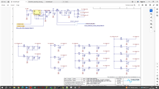
    On 2 unit we are seeing current fluctuation of about 30mA after every 4-5 sec on VCC1_VCO voltage. I have attached out circuit schematic of voltage rails and 2 videos to show the behavior of power supply with and without VCC1_VCO connected.

    • 1st video shows the current when L32 choke is removed and as per our schematic design (shown below) that takes out all three VCC1, VCC5, and VCC6 voltage rail and result you can see in video that current is stable at 670mA.
    • 2nd video shows the current when L32 is placed but R642 is removed and as per our design schematic it only removes the VCC1 and the result is shown in video that there is fluctuation of 30mA is happening and we do not know what causing VCC1_VCO to draw 30mA current.

    Thanks for your help,

    1st video:

    2nd video:

    LMK04828B Power supply schematic page

    Regards,

    Arshad

  • Am I understanding correctly that in both videos, one or more LMK04828 supply pins are disconnected? All device power supply pins must be connected to a nominal 3.3V supply or the device will not operate properly, and the behavior with one or more power supply pins disconnected is undefined. Please correct me if I'm misunderstanding.

    If you are asking about why a particular behavior occurs in an invalid usage mode, I doubt I could offer you an insightful or useful answer. My wild guess would be there is some small, periodic leakage through unpowered elements that is slowly charging the VCC1_VCO rail enough to trigger some POR circuit, which quickly depletes the available charge; and that this condition is only present when VCC1_VCO is unpowered but other rails are powered. You could probe the capacitor voltage across VCC1_VCO in the case where R642 is removed to observe if this is occurring. But again, this is not a valid usage of the LMK04828, so there could be many other reasons.

  • yes, it's right and it is only to do root cause analysis to check which of the pins are actually causing this sudden increase of current.

    Sorry for confusion, actually as shown in video 2, when this fluctuation occurs all three VCC1, VCC5, and VCC6 are connected and hence see this fluctuation.

    and video 1 shows the condition when VCC1 is disconnected and both VCC5 and VCC6 are still connected and result is there is no fluctuation in current.

    which suggests that VCC1 is causing this current spikes when connected.

    Hope it is more clear now.

    Thanks

  • Okay, that makes more sense.

    Normally, there should be virtually no spikes in DC current once the device is locked. Usually a spike in current from connecting the VCO means the VCO is not locked and is drifting in frequency. But it could also be a result of clocks derived from the clock distribution frequency (such as the SYSREF) causing unintended behavior, such as continuously resetting dividers with SYSREF active and SYNC_DISx bits set to 0.

    Here's a few theories:

    • Temporary loss of lock: maybe PLL2 is losing lock for a short period. You could monitor the lock detect signal or the CPout2 pins to look for loss of lock. You could check CPout2 voltage on an oscilloscope to see if it remains stable at around 1.2V. You could check the PLL2_R and PLL2_N signals (or rather their divided-down copies) on the status pins to debug if the R or N signals are doing anything strange.
    • Building on possibility above: We discussed your loop filter for PLL1, but maybe PLL2 needs review - I've seen a few times where people try to include external third and fourth order components without realizing these are integrated, for example, which can occasionally destabilize the loop filter.
    • Since the SYNC and SYSREF distribution path are shared, if the SYSREF is resetting dividers, this could look like a large spike in current that is aliased with the sampling interval of the current measurement on the power supply. I'd expect this to be happening on every board, so I don't think this is the root cause. But I could take a look at the register settings regardless, as this might turn something up.
    • Another register settings possibility: if PLL2_N_CAL is not programmed correctly, the VCO might be calibrated incorrectly. This can cause some, but not all, devices to have marginally stable lock at some conditions based on process variation in the VCO. VCO calibration is triggered by writing the LSBs of PLL2_N, so PLL2_N_CAL should be programmed before writing the LSBs of PLL2_N; during calibration, the value of PLL2_N_CAL is temporarily substituted into PLL2_N, and the prescaler -> N divider path is selected for calibration, so PLL2_PRE_PD must be 0 to enable the prescaler path and VCO_Freq / (PLL2_PRE * PLL2_N_CAL) must equal PLL2_Fpd.
    • Similar issue: if writing all registers in ascending order, PLL2_N LSBs are written before enabling the PLL supplies, so the PLL may not be on when calibration is triggered. Make sure PLL2_N is written after the other registers. The register export function of TICS Pro should automatically arrange for the relevant register to be written last (or close to last).
    • If the LDObyp1 and LDObyp2 pins don't have the recommended bypass capacitor values in the datasheet (10μF and 0.1μF respectively), this could cause the internal VCO LDO to be unstable or marginally stable.
    • Maybe you just have bad luck: something isn't soldered properly, the unit might have been damaged, the board might have an issue, etc. Let's look at stuff that's easy to debug and fix first like loop filter, register settings, loss of lock; but if nothing else turns up, reseating the device might resolve the issue, or AB-swapping a known-good device could help narrow down the issue to specific devices or boards.
  • One more possibility I just thought of: it looks like you're using a switching supply for the LMK04828 power supply. This might be injecting switching noise onto the PLL1 charge pump or the VCXO, which could be making a big enough spur to cause lock issues. Most other LMK04828 supply pins have LDOs on them, but PLL1 charge pump is basically direct from the supply pin, so it may be coupling a switching spur onto the VCXO... In practice this usually isn't an issue except with really high ripple, because the PLL1 loop filter tends to roll off the switching noise, but if the ripple is large enough it might be a problem. And it could be a direct spur injection on the VCXO supply, which again wouldn't affect PLL1 much due to the narrow bandwidth, but which might affect PLL2 significantly more since the spur from the switcher is closer to in-band (only about an order of magnitude away). You could try bypassing the switching supply with an off-board power supply.

  • Hi Derek, 

    thank you for the reply,

    I think it is more of an issue when VCO is not locked, as the current spike goes away after few mins (approx 10-15 mins). and then unit draws 930mA current without any fluctuation in it.

    Really appreciated you input into this and will look into try with bypassing the switching supply with off board PSU and see if it resolve the issue.

    Thanks,

    Arshad