LMK04832: Clock Architect buffer output power question

Part Number: LMK04832
Other Parts Discussed in Thread: LMK04610, LMK01000

Tool/software:

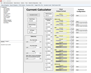
is the power number listed for my LMK04832 configuration in Clock Architect only the Core power or does this include the outputs power as well? I cannot tell if the LVPECL and LVDS currents that get sourced to their loads are taken into account here. 

  • Hi KEvin, 
    Please use TICSpro to estimate current consumption for given configuration: 

    Best regards, 

    Vicente

  • I configured the chip in TICSpro to bypass and disable PLL0 and PLL1 and just act as a buffer like what the Clock Architect came up with and the overall power is around 1.2W. How can this be? Clock Architect stated the power was only around 366mW

  • Hi Kevin, 
    That does not sound correct. 
    In my case - the current calculator is showing around 300mA of current. 
    Which does seem accurate. 
    1W of power sounds about right. 

    I will report the bug to our AE in charge of clock tree architect. 

    Best regards, 

    Vicente 

  • The discrepancy may be because I am also including the current for the LVPECL emitter bias resistors of 240 ohms. Either way, 1 to 1.1W is too much power for what I am trying to do. I am now looking at LMK01000 to generate Three 200MHz clocks and Two 1MHz SYSREF clock signals (all LVPECL with emitter resistors). I arrive at a power calculation of 778mW. Do you concur? Is there another clock chip that could be even less power? Why do so many other parts in TICsPro not have power/current calculators like the LMK04832 does? It's possible the LMK04610 in PLL Bypass mode is even lower powered than the older LMK01000 but I do not know how to calculate the power for that one since it does not have a current calculator in TICsPro and the datasheet does not break down the power for bypass mode. 

  • Hello,

    The team is out for the holidays. Please expect a response by Jan 2 at the earliest.

    Thanks,

    Kadeem

  • Hello Kevin, 
    LMK01000 is a clock buffer and the two 1MHz SYSREF clocks will be continuous signals - I just want to be sure this is acceptable for your application. 
    Older devices don't have the current calculator as many of our parts are low power parts where the requirement for power calculation wasn't really needed. 
    That is no longer the case - this is even more true on our power hungry RF synthesizers and dividers. 
    I arrived at ~740mW of power dissipated. 
    Can I have more information about your application - What is the maximum current consumption for your application? LVPECL is usually the most power hungry differential output format. 
    Would you be open to using LVDS or any other differential output format? 

    Best regards ,

    Vicente 

  • Most of the outputs can be LVDS as I indicate in this drawing, however, two of the clocks and the SYSREF they are paired with have to be a differential swing closer to what LVPECL is - LVDS will not work. The RFSoC can adjust the setup time of SYSREF to CLK at the input. So as long as the output-to-output skew of adjacent clock outputs from the buffer are small (relative to the period of the 200MHz clock) and repeatable, then a clock buffer with dividers should work.

  • Hi Kevin, 
    I'm afraid given the number of outputs you have you're limited to a jitter cleaner. 
    I do believe LMK3H2018 might suffice given it has a buffer mode option, but I would need to check if we can divide down a 200MHz input - and most importantly do we meet your power consumption requirements. 
    Is there a specific power dissipation number you need to meet?