This thread has been locked.

If you have a related question, please click the "Ask a related question" button in the top right corner. The newly created question will be automatically linked to this question.

LMK03328: LMK03328 low probability no output

Part Number: LMK03328

Tool/software:

Hello, TI's technical experts!

We have a project that uses LMK02338,as the input clock for FPGA and ADC.

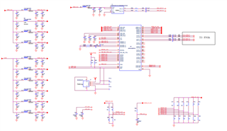
This project has been mass-produced. There is a low probability (0.5%) that LMK02338 has no output. The schematic diagram is as follows.

The tests we have done on PCBA are as follows:

1. Power: vdd=3.3V, VDDO=1.81V

2. Pin6/7(clk): 100MHz, vpp=137mv

3. Pin13 (PDN) reset timing:
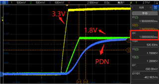
We found that the chip can be restored to normal by manually pulling down and then pulling up PDN; it can also be restored to normal by resetting through I2C software control;

In addition, we found that the problem is easy to reproduce if the PCBA is left alone for several hours and then powered on.

The support we need is as follows:
1. Please help check whether the schematic diagram is correct
2. What are the possible causes of this problem and from which aspects should it be analyzed?

Hope to hear from you soon,Thank you for your support!
  • Benson,

    Our team is currently out of office for the US holiday. Please expect a response by next Monday.

    Thanks,

    Kadeem

  • Benson,

    I don't see any issues with the schematic. Can you provide an i2c dump of the part when it's functioning normally and when it's in the error state? 

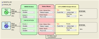
    Additionally, if you change STAT0 to be PLL1LOL, what is the level of the STAT0 pin when the device is experiencing the issue?

    In addition, we found that the problem is easy to reproduce if the PCBA is left alone for several hours and then powered on.

    Have you tested this over temperature as well?

    Best,

    Cris

  • hi cris,

    Thank you for your reply.

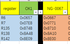
    The following are the register values ​​in the error state.

    Compared with the registers of the normal PCBA, R6/R7 and R135/R138/R142 are different, and the other register values ​​are the same.

    Can these register values ​​provide some analysis direction?

    R0 0x0010
    R1 0x010B
    R2 0x0232
    R3 0x0302
    R4 0x0401
    R5 0x0501
    R6 0x0667
    R7 0x0771
    R8 0x0802
    R9 0x0900
    R10 0x0AA8
    R11 0x0B00
    R12 0x0CD9
    R13 0x0D00
    R14 0x0E00
    R15 0x0F00
    R16 0x1000
    R17 0x1100
    R18 0x1200
    R19 0x1303
    R20 0x1455
    R21 0x1555
    R22 0x1600
    R23 0x1703
    R24 0x1800
    R25 0x19F5
    R26 0x1A00
    R27 0x1B20
    R28 0x1C50
    R29 0x1D0F
    R30 0x1E7A
    R31 0x1F24
    R32 0x2024
    R33 0x2103
    R34 0x2220
    R35 0x2320
    R36 0x240F
    R37 0x2512
    R38 0x2601
    R39 0x2711
    R40 0x280F
    R41 0x2910
    R42 0x2A0F
    R43 0x2B10
    R44 0x2C0F
    R45 0x2D0F
    R46 0x2E00
    R47 0x2F00
    R48 0x30FF
    R49 0x310A
    R50 0x329A
    R51 0x3303
    R52 0x3400
    R53 0x3500
    R54 0x3600
    R55 0x3700
    R56 0x3810
    R57 0x3908
    R58 0x3A00
    R59 0x3B32
    R60 0x3C00
    R61 0x3D00
    R62 0x3E00
    R63 0x3F00
    R64 0x4000
    R65 0x4101
    R66 0x420C
    R67 0x4310
    R68 0x4400
    R69 0x4578
    R70 0x4600
    R71 0x471D
    R72 0x4818
    R73 0x4900
    R74 0x4A32
    R75 0x4B00
    R76 0x4C00
    R77 0x4D00
    R78 0x4E00
    R79 0x4F00
    R80 0x5001
    R81 0x510C
    R82 0x5210
    R83 0x5301
    R84 0x5404
    R85 0x5507
    R86 0x5600
    R87 0x5700
    R88 0x5800
    R89 0x59E3
    R90 0x5A01
    R91 0x5B32
    R92 0x5C01
    R93 0x5D59
    R94 0x5E01
    R95 0x5F9C
    R96 0x6001
    R97 0x61EE
    R98 0x6202
    R99 0x632E
    R100 0x6402
    R101 0x65A4
    R102 0x6603
    R103 0x670A
    R104 0x6801
    R105 0x699C
    R106 0x6A05
    R107 0x6B00
    R108 0x6C08
    R109 0x6D0F
    R110 0x6E1F
    R111 0x6F00
    R112 0x7000
    R113 0x7100
    R114 0x7200
    R115 0x7308
    R116 0x7419
    R117 0x7500
    R118 0x7607
    R119 0x7701
    R120 0x7800
    R121 0x7900
    R122 0x7A08
    R123 0x7B0F
    R124 0x7C1F
    R125 0x7D00
    R126 0x7E00
    R127 0x7F00
    R128 0x8000
    R129 0x8108
    R130 0x8219
    R131 0x8300
    R132 0x8407
    R133 0x8501
    R134 0x8600
    R135 0x8710
    R136 0x8802
    R137 0x8910
    R138 0x8A10
    R139 0x8B00
    R140 0x8C00
    R141 0x8D00
    R142 0x8E00
    R143 0x8F00
    R144 0x9000
    R145 0x9100
    R169 0xA940
    R172 0xAC24
    R173 0xAD00

  • Benson,

    Compared with the registers of the normal PCBA, R6/R7 and R135/R138/R142 are different, and the other register values ​​are the same.

    Thank you for the information. Just to confirm, are the two register dumps being compared in the table from different parts? The registers that are different between the two are device specific (Part ID values, etc). 

    From the full register list you provided, I have found no issues with the config on the bench, and the registers do not indicate any problems with the device. 

    Can you conduct an ABA swap (putting a failed part on a known good board and a known good part on a failed board) and see if the issue follows the device or the board? This will greatly help narrow down the possibilities.

    Best,

    Cris

  • Hi Cris,

    Regarding the previously reported issue with LMK03328 having a low probability (0.5%) of no clock output, we have made some new progress:

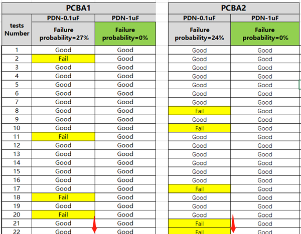
    We changed the PDN capacitor from 0.01µF to 1µF, which increased the PDN delay and effectively improved the issue of no clock output.

    The following is a statistical comparison of the data of the two problematic PCBAs before and after adding PDN delay.


    I have two questions that need your help to answer:

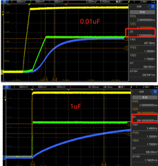
    1. Before increasing the delay, the PDN delay(0.01uf) was already ≥1ms. Why did the low-probability no-clock-output problem still occur? What is the theoretical value for this delay?

    2. After changing the PDN capacitor to 1µF, the delay has increased to ≥200ms. Does the LMK03328 have any requirements for the maximum delay? We have verified that this change does not affect product application.

    Thank you very much for your support!

  • One more thing to add: PDN capacitor changed from 0.01uF to 1uf, PDN power-on timing delay comparison chart

  • Hello,

    The team is out for the holidays. Please expect a response by Jan 2 at the earliest.

    Thanks,

    Kadeem

  • Hi Cris

    Happy new year!

    I'm not sure if I have disturbed your vacation?

    The problem of occasional clock output failure mentioned above,After we increased the power-on PDN delay, the problem did not occur again after multiple tests. Please also help answer the two questions mentioned above,


    Thank you very much for your support!

  • Benson,

    To be clear: After increasing the PDN delay, no issue was observed?

    Theoretically, there should be no issue with PDN reaching 1.2V 1ms after the VDD and VDDO voltages have stabilized. In practice, I recommend using a value of 0.1uF minimum when using split supply rails to relay the PDN ramp until the supply voltages (and therefore, any internal device LDOs) are definitively stable.

    There is not any maximum delay specification between the ramp of the supply voltage pins and the ramp of the PDN pin. We have tested multiple configurations with a PDN ramp delay of several seconds without issues.

    Thanks,

    Kadeem

  • Hi Kadeem,

    We have tested repeatedly and confirmed that increasing the delay can indeed solve this problem.


    Thank you very much for your support!