- Ask a related questionWhat is a related question?A related question is a question created from another question. When the related question is created, it will be automatically linked to the original question.
This thread has been locked.
If you have a related question, please click the "Ask a related question" button in the top right corner. The newly created question will be automatically linked to this question.
Tool/software:
Hi Ti team,
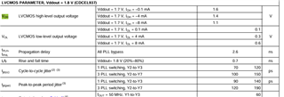
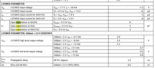
Im planning to use the CDCEL937QPWRQ1 clock buffer with Input oscillator of 27Mhz & 6 output clock as 27Mhz, the supply & output voltage of 1.8V. While doing DC analysis there are VOH, VOL values for multiple source & sink current. The receiver side 6x clock inputs source & sink current is not given in the datasheet. In that condition which VOH, VOL values to be considered or do we have any options to calculate the Source & sink currents.
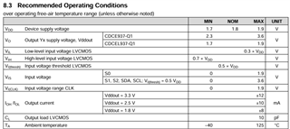
6x clocks will be given to a sensor which has Vih=0.7*1.8=1.26V, VIL=0.3*1.8=0.54V
Please let me know.

Syed,
This result is for the case of all seven outputs buffered from the input. My recommendation is to model your setup using the CDCE913 IBIS model to ensure that you will not have issues: https://www.ti.com/lit/zip/scam056
Thanks,
Kadeem
Hi Kadeem,
Thanks for the reply
Unfortunately I'm not familiar with the IBIS modeling. Can we have any other option to identify the source and sink current details.
Hi Kadeem,
I have raised query with sensor vendor for the input impedance of the clock pins,
Meantime i would like to confirm that the input capacitance 6pf in datasheet indicates the input clock pin capacitance Xin of the IC which must be met from an external Oscillator (in my case Im using oscillator not crystal).
And the output load of LVCMOS indicates the 10pf is the max load this IC can drive at output side on each clock channels.
is my understanding correct? could you please clarify.
In my design, this IC will have 15pf oscillator at input side & 6x clock outputs will be connected to 6 sensors. the sensor input capacitance is still not available.


Syed,
The input capacitance spec is the load the IC will present to the oscillator.
The output load is not the max the part can drive, but it is the max capacitance that all the relevant parameters are guaranteed. For example, a higher capacitance will end up drawing more current and the slew rate will be reduced, but there will still be an output present. Though eventually, enough capacitance *will* impact the VOH and VOL achieved at a certain frequency.
So if the oscillator is can drive 15 pF, the IC will present a much lighter load to the oscillator. And the output driving more than 10pF may be fine depending on factors such as the frequency, the minimum required slew rate, and the operating temperature.
Best,
Cris