This thread has been locked.

If you have a related question, please click the "Ask a related question" button in the top right corner. The newly created question will be automatically linked to this question.

LMK5C33216: LMK5C33216

Part Number: LMK5C33216

Tool/software:

hi

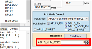
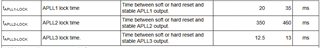
I am using TI LMK5C33216 at my design and looking for more information regarding the phase lock mechanism, i would like understand the following:

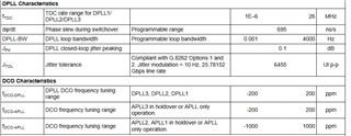
1. where can I find more information regarding the phase lock circuit? maybe any application note?

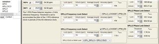
2. in case of LOPL, does the device restart acquiring of the input similar to what is performed in case of  LOFL ( move to holdover and .....).

3. For having output clock phase that is fixed to the input, I must use the ZDM, correct?

4. incase that the input clock phase is changing what will be the behavior of the output clock assuming I don't see LOPL?

Thx,

Haim


  • Hi Haim,

    We recommend using the newer and improved version called the LMK5C33216A. This has better jitter performance and adds HCSL functionality. The pin out stays the same but there are some registers that change.

    1. We currently do not have a separate app note; the only information on LOPL is on the datasheet. What details were you looking to see?
    2. The device does not restart if LOPL=1. The device enters holdover when the DPLL reference is no longer consider valid such as due to improper frequency or amplitude.
    3. When the DPLL is locked (LOPL=0, LOFL=0), the outputs are phase aligned to the DPLL input. If ZDM is enabled, then the outputs share a deterministic phase relationship with the DPLL inputs which means that upon a PDN or software reset, the input to output phase difference is the same/constant/fixed.
    4. If the DPLL is frequency locked (LOFL=0) but nt phase locked (LOPL=1), then the output may not have the same phase as the input but they will have the same frequency accuracy as the inputs.

    Does this help?

    Regards,

    Jennifer

  • Hi Jennifer,

    thanks for the fast response.

    At case that the DPLL is freq lock (LOFL=0), lets say that after some time the input clock phase move out of the threshold (LOPL=1) but freq remine the same (LOFL=0), is it correct to say that at this case nothing will happen and the input phase will transferred to the output and only in case of frequency change the device will move to holdover. is that right?

    when working with ZDM and the only change will be with input clock phase, what will be the output phase ?

    please advise,

    Thx,

    Haim

  • Hi Haim,

    Happy New Year!

    If the DPLL reference is considered a valid reference, LOFL=0, and LOPL=1 during normal operation, the DPLL will remain active and continue tracking the input. The device moves to holdover if the DPLL reference becomes invalid such as due to a missing reference or unexpected frequency measured by the device.

    It is possible for the outputs to be phase locked to the input but the device still report LOPL=1. This can occur when the LOPL thresholds are low. For example, if the lock LOPL threshold is set to 1 ppm, then the LOPL status signal will not clear until the error between the DPLL input and the VCO output is less than 1 ppm. When the DPLL is active, the DPLL continuously updates the APLL numerator until a near 0 ppm error is achieved between the input and outputs.

    As mentioned, the device offers ZDM to provide deterministic input to output phase relationship which means the phase error is always known even after a power down/software reset. After identifying such deterministic error, a DPLL phase offset can be applied (through register setting) to zero out the phase error between the input and output. If the DPLL is locked, but the input has a phase change, then the outputs also get the phase change so the outputs remain phase aligned to the input. Does that make sense?

    Regards,

    Jennifer

  • Hi Jennifer,

    Happy new year Slight smile

    your answer make sense, so i would like to understand the following:

    1. can I set the Jitter cleaner to ignore input clock phase change (output will not track input clock phase) and only track the input freq?

    2. as you wrote the "DPLL continuously updates the APLL numerator until a near 0 ppm error is achieved between the input and outputs." can I read this value constantly?

    also can I read the phase difference between input clock to DPLL measurement? 

    3. I didn't find at the programming guide where to set the LOPL threshold, can you point to the relevant reg ?

    Regards,

    Haim

  • Hi Haim,

    1. Let me check this with the team if this is possible. Most applications require the outputs to track the input's phase and frequency.
    2. Yes, there is a readback register to read the live APLL numerator value, called APLLx_NUM_STAT (R862 to R858 for APLL3). Regarding the phase difference readback, it is also possible to read the TDC value (phase error between the input and VCO feedback output clock).
      1. APLL NUM STAT in TICS PRO:
    3. We recommend using the TICS Pro Software to determine the proper LOPL register settings for your application. Choose the LMK5C33216A profile for LMK5C33216A devices and fill in the details in the Start Page.
      1. Refer to the TICS Pro walkthrough videos at the bottom of the TICS Pro download page:
      2. The LOPL/LOFL settings in terms of ppm can be found in the Validation page.

    Regards,

    Jennifer

  • Hi Jennifer,

    1. waiting for your feedback regarding item previous 1.

    2. can you share graph that show output phase as function of the device temperature (wondering if it have any affect).

    3. can you advise if all 3 DPLL have same performance.

    Regards,

    Haim

  • Hi Haim,

    1. Regarding 1, it is not possible to separate the phase from frequency. Can you please elaborate your use case? What application requires the phase to stay fixed and only follow the frequency accuracy?
    2. We do not have a graph of phase over temperature available. The device has been tested over -40 deg C to 85 deg C, such validation results are listed in the datasheet. I will say that the XO input performance impact the output phase noise performance for phase noise offsets less than 1 kHz. If the XO input is susceptible to temperature change, then the XO can impact the wander noise performance. A TCXO or OCXO is recommended if the application is sensitive to temperature variations and wander noise.
    3. What performance do you mean? Locking capabilities? Noise? Everything?
      1. The DPLLs have the same capabilities and features but may vary for certain things due to different VCOs for each DPLL+APLL pair. For example, the DCO step size is different but the TDC range is the same per datasheet:
      2. Also, the APLL lock time can be different due to the different VCO found in each APLL, which can affect the DPLL lock time.

    Regards,
    Jennifer