This thread has been locked.

If you have a related question, please click the "Ask a related question" button in the top right corner. The newly created question will be automatically linked to this question.

LMX2594: External 10MHz Clock Implementation on LMK04828 on RFSoC4x2

Part Number: LMX2594
Other Parts Discussed in Thread: LMK04828, USB2ANY,

Tool/software:

Hi Team,

Can you please help us with our customer inquiry below.

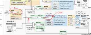
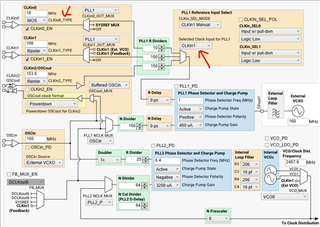
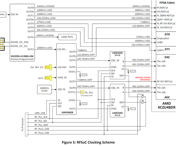
We are trying to enable CLK_IN_0 (image 1) to have a 10MHz signal sync with the device. Looking at TICS and PYNQ forums

https://discuss.pynq.io/t/xrfclk-configuration-lmk04828-using-external-10mhz-reference-clock/5562/12
 
https://e2e.ti.com/support/clock-timing-group/clock-and-timing/f/clock-timing-forum/1229913/lmk04828-taking-driving_clock-from-another-input-pin-and-i-can-t-figure-out-which-one/4661353#4661353 

I came across 3 different solutions. Provided are .txt files for hex import for each. Using TICS PRO, I am trying to configure our board to have a 10MHz external clock control while disabling OSCin internal referance clock. The other frequencies on the image should remain the same. I don't want to program the board by using USB2ANY cable with any of these .txt files for hex import because we don't have the default LMK04828 .tcs file for the RFSoC4x2. Can you please help us on how we can proceed? We are really stuck and Real Digital didn't provide us the default LMK04828 file for the board. 

Regards,

Danilo

  • Let me try to understand this:

    1.  You are using a 3rd party board that has the LMK04828

    2.  You are not sure what the settings are for this board for the LMK04828

    3.  If you knew the settings for the LMK04828, then you could use TICSPRO, but provider of the board (Real Digital), is not giving you this information.

    With TICSPRO, you can export and import hex registers to other tools and this does not require you to have TICSPRO hooked up to the board.  If TICSPRO is hooked up to the board, you can also read back the register states.  

    Or if you are asking for a configuration file based on the frequencies in the above diagram, we can provide that.  However, to do this we need:

    With your frequencies, I think you want the VCO to be 2949.12.  You could use the 160 MHz OSCin value, but this will lead to a very low phase detector frequency, which will work, but yield not very good perforamnce.  It would perform much better with a differetn OSCin frequency like 122.88, but this is a hardware change.

    Regards,
    Dean

    Regards,

    Dean

  • Hi Dean,

    Please see our customer's response below.

    Thank you for your answer,
    1. We are using RFSoC4x2 board, we are tying to eliminate the phase delay for ADC-DAC signal processing by locking the phase with a signal generator at 10MHz from Ext. Ref. Clk. (CLK IN0)
    2. We don't know the default LMK04828 for this board apart from the data sheet provided in Figure 5.
    3. We connected USB2ANY to the board and read the register values however, they didn't match with what they have on Figure 5. We think that is possible since USB2ANY doesn't connect directly to LMK but instead to Skyworks Si5395.

    Therefore I don't think we can modify OSCin Value of the boards. The frequency requirements are clkin0 should be 10MHz, clkin1 should be 100MHz, OSCin should be 160MHz.
    The clkouts of LMK should be same with figure 5 provided in my initial question. It would be great if you can provide a .tcs file with this requirements, we are new to TICSPro and not sure if the following work.
    Currently, our design is as follows:
    CLK_in & PLLs
    CLK Outputs:
    I want to double check if this design would work before writing it to LMK since we don't have the register values. Thank you for your answer.
     
    Regards,


    Danilo
  • Hi Danilo,

    first of all, although the board was not design by our customer, I have doubt to the block diagram.

    7.68MHz clocks have to be generated by the SYSREF block of LMK04828, as the clock divider is not big enough to support 7.68MHz. This is fine as long as the SYSREF block is configured as Continuous SYSREF output.

    OUT4 and OUT1 are used as the SYNC signal to LMX2594, SYNC signal is a single pulse so it also have to be generated by the SYSREF block of LMK04828. However, in this case, the SYSREF block needs to be configured as Pulser mode. 

    That means, OUT3 and OUT9 will be a pulse instead of continuous clock when we attempt to synchronize the LMX2594 devices. 

    Back to the LMK04828 configuration, here is the configuration.

    The 10MHz clock needs to be square wave, otherwise PLL1 may not lock. Use a square wave clock and set the input type to MOS. 

    Use the register next to PLL1 R Dividers to select CLKin1 or CLKin0.

    Configure SYSREF to Continuous clock mode.

    example output configuration, you may need to select the correct output format based on the board design.

    here is the tcs file.

    7652.lmk04828.tcs

  • Hi Danilo,

    To add to what Noel said, in order to achieve phase synchronization between the input and output signals, you will have to put the device into zero-delay mode. I have attached a tcs file that does that, you will just need to update all of the outputs as you see fit. However, the phase noise performance will be suboptimal due to the numbers that the configuration will have to support - as Dean mentioned, it would be better if the VCXO frequency were 122.88 MHz.

    lmk04828_rfsoc.tcs

    Furthermore, in order to achieve the deterministic phase relationship between the input and output, you will need to generate a SYNC event. Section 9.7.3.10 provides an overview of how to generate one. The SYNC event results in all of the output dividers being phase aligned, and you will have achieved your necessary clock tree and input output relationships.

    Thanks,

    Michael

  • Hi Noel and Michael,

    Thank you for your help. We have 3 more questions regarding this. I modified the zero-delay rfsoc file to match with our required clock output values and also enabled continuous SYNC for deterministic phase relationship. Here is how it looks right now.

    We have a few more questions.

    1- The first .tcs file you provided has a different internal VCO clock compared to the zerodelay .tcs file. (2457MHz / 2949MHz). As long as the output clocks have the right frequency, does the internal VCO clock's frequency matter?

    2- I modified SYNC/SYSREF to be in continuous SYSREF mode referencing from the section you mentioned, I think this mode should continuously align the phases. Also, the selected clock input for PLL1 should be CLK0 since that's where the signal generator's 10MHz will be connected. Are these right assumptions?

    3- PLL1 and PLL2 are both locked in this configuration. Before continuing to test this .tcs file with our RFSoC4x2 board and signal generator. Is it possible for you to check/verify the accuracy? I attached .txt file for raw register values. Real Digital doesn't reply back to our emails. We want to make sure to have the correct configuration.

    6303.HexRegisterValues.txt
    R0 (INIT)	0x000090
    R0	0x000000
    R2	0x000200
    R3	0x000306
    R4	0x0004D0
    R5	0x00055B
    R6	0x000600
    R12	0x000C51
    R13	0x000D04
    R256	0x01000C
    R257	0x010155
    R258	0x010255
    R259	0x010301
    R260	0x010422
    R261	0x010500
    R262	0x0106F0
    R263	0x010711
    R264	0x01080C
    R265	0x010955
    R266	0x010A55
    R267	0x010B00
    R268	0x010C22
    R269	0x010D00
    R270	0x010EF0
    R271	0x010F10
    R272	0x01100C
    R273	0x011155
    R274	0x011255
    R275	0x011300
    R276	0x011422
    R277	0x011500
    R278	0x0116F1
    R279	0x011701
    R280	0x011818
    R281	0x011955
    R282	0x011A55
    R283	0x011B00
    R284	0x011C02
    R285	0x011D00
    R286	0x011EF1
    R287	0x011F33
    R288	0x012018
    R289	0x012155
    R290	0x012255
    R291	0x012300
    R292	0x012422
    R293	0x012500
    R294	0x0126F0
    R295	0x012711
    R296	0x01280C
    R297	0x012955
    R298	0x012A55
    R299	0x012B00
    R300	0x012C02
    R301	0x012D00
    R302	0x012EF9
    R303	0x012F00
    R304	0x01300C
    R305	0x013155
    R306	0x013255
    R307	0x013300
    R308	0x013402
    R309	0x013500
    R310	0x0136F9
    R311	0x013733
    R312	0x013820
    R313	0x013903
    R314	0x013A01
    R315	0x013B80
    R316	0x013C00
    R317	0x013D08
    R318	0x013E03
    R319	0x013F11
    R320	0x014009
    R321	0x014100
    R322	0x014200
    R323	0x014333
    R324	0x01447F
    R325	0x01457F
    R326	0x01460B
    R327	0x0147BA
    R328	0x014812
    R329	0x014952
    R330	0x014A02
    R331	0x014B16
    R332	0x014C00
    R333	0x014D00
    R334	0x014EC0
    R335	0x014F7F
    R336	0x015003
    R337	0x015102
    R338	0x015200
    R339	0x015300
    R340	0x01540A
    R341	0x015500
    R342	0x015601
    R343	0x015700
    R344	0x015801
    R345	0x015900
    R346	0x015AA0
    R347	0x015BD4
    R348	0x015C20
    R349	0x015D00
    R350	0x015E00
    R351	0x015F0B
    R352	0x016007
    R353	0x0161D0
    R354	0x016284
    R355	0x016300
    R356	0x016424
    R357	0x016500
    R369	0x0171AA
    R370	0x017202
    R380	0x017C15
    R381	0x017D33
    R358	0x016600
    R359	0x016706
    R360	0x016800
    R361	0x016959
    R362	0x016A20
    R363	0x016B00
    R364	0x016C00
    R365	0x016D00
    R366	0x016E13
    R371	0x017300
    R386	0x018200
    R387	0x018300
    R388	0x018400
    R389	0x018500
    R392	0x018800
    R393	0x018900
    R394	0x018A00
    R395	0x018B00
    R8189	0x1FFD00
    R8190	0x1FFE00
    R8191	0x1FFF53
    

    Regards,

    Danilo

  • Hi Danilo,

    1. Preferably, you would use 2457.6 MHz as your VCO frequency, as this will require a lower N divider value, which will reduce the phase noise.

    2. Continuous SYSREF (while the correct SYSREF configuration)will not automatically align the phases, you must perform a SYNC event to achieve that. Also, yes, you should select CLKin0 as the driver of PLL1 if that is the input for the 10 MHz signal. 

    3. I cannot test your exact configuration on my board, as our evaluation boards come with 122.88 MHz VCXOs attached. However, I can confirm that both of your PLLs lock. I downloaded your configuration and tested it (albeit with different numbers for the first PLL, but with numbers that have the exact relationship as in your configuration) and found that both PLLs will lock. 

    I have attached the final configuration for good measure. Hope this helps.

    rfsoc_lmk4828.tcs

    Thanks,

    Michael