This thread has been locked.

If you have a related question, please click the "Ask a related question" button in the top right corner. The newly created question will be automatically linked to this question.

LMK04828: Couldn't able to figure out how to get register space for LMK04828 to get desired output clocks

Part Number: LMK04828
Other Parts Discussed in Thread: LMK04832

Tool/software:

Hi Team.

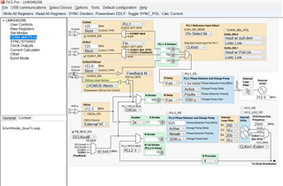
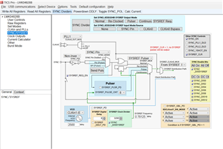
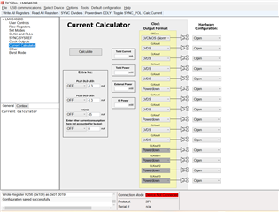
We are working on  ADC - DAC Loopback on  FMC Evaluation board, which is having a clock generator - LMK04828 & a transceiver on it.

For this we need a register dump (register write sequence) to configure the LMK04828 to get the desired clocks.

We need the following clocks with mentioned frequencies to configure on LMK04828:

DCLKOUT0, DCLKOUT0* = 100 MHz

SDCLKOUT1, SDCLKOUT1* = 100 MHz

DCLKOUT6, DCLKOUT6* = 125 MHz

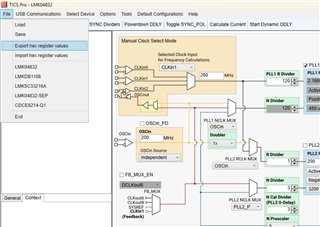
NOTE : We are using OSCIN (Pin 43 of LMK04828) as the reference clock(which is 48 MHz clock oscillator) for LMK04828.

We are attaching the LMK04828 IC chip Image for reference.

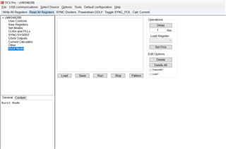
We require the register dump for LMK04828 to configure the above clocks to implement the ADC - DAC loopback for our requirement.

Please kindly proved us the register dump (register write sequence) like 0x000090 where MSB 2 Bytes 0000 represents address of register & LSB Byte represents Data to write into that particular register.

We will look forward for your reply.

  • Hi Lamski, 
    I also see CLKinX is utiltized as well as CPout1 referencing a VCXO. 
    This implies to me the VCXO outputs 48MHz. 
    What is the CLK signal at CLKIN0 which is used as reference for PLL1? 


    If you could also provide a clock tree that would be useful. 

    Please note we have a tool, TICSpro, which is capable of doing this. You create you configuration file and can export as a hex file with all registers and their contents for use with your driver. 

    Best regards, 

    Vicente 

  • Hi Vicente flores prado,

    We are not using CLKIN0 as reference clock for LMK04828 whereas we are using OSCIN (48 MHz) as a reference clock.

    We don't aware how to configure different configurations tabs in TICS Pro software to generate thee register space.

    We are attaching the screenshots of LMK04828 in TICS Pro Configurations tabs below.

    1) User controls

    2) Raw Registers

    3) Set Modes

    4) CLKin and PLLs

    5) SYNC/SYSREF

    6) Clock Outputs

    7) Current Calculator

    8) Other

    9) Burst Mode

    We need the following clocks with mentioned frequencies to configure on LMK04828:

    DCLKOUT0, DCLKOUT0* = 100 MHz

    SDCLKOUT1, SDCLKOUT1* = 100 MHz

    DCLKOUT6, DCLKOUT6* = 125 MHz

    Please kindly help us how to configure all these 9 configurations tabs in TICS Pro Software to get the above desired output clocks with mentioned frequencies.

    We will look forward for your reply.

    Thank You.

  • Hi Vicente flores prado,

    And also, we actually have a register dump which we are currently using (for sampling rate 122.88 MHz), in vitis to program LMK04828.

    Now actually we have to change frequencies of some output clocks of LMK04828.

    We are attaching that register dump below.

    .

    0x000090,
    0x000010,
    0x000200,
    0x000306,
    0x0004D0,
    0x00055B,
    0x000600,
    0x000C51,
    0x000D04,
    0x010019,
    0x010155,
    0x010255,
    0x010300,
    0x010400,
    0x010500,
    0x0106F0,
    0x010711,
    0x010819,
    0x010955,
    0x010A55,
    0x010B00,
    0x010C20,
    0x010D00,
    0x010E70,
    0x010F11,
    0x011019,
    0x011155,
    0x011255,
    0x011300,
    0x011420,
    0x011500,
    0x0116F0,
    0x011710,
    0x011819,
    0x011955,
    0x011A55,
    0x011B00,
    0x011C00,
    0x011D00,
    0x011E70,
    0x011F01,
    0x012019,
    0x012155,
    0x012255,
    0x012300,
    0x012400,
    0x012500,
    0x0126F1,
    0x012700,
    0x012819,
    0x012955,
    0x012A55,
    0x012B00,
    0x012C00,
    0x012D00,
    0x012E79,
    0x012F00,
    0x013019,
    0x013155,
    0x013255,
    0x013300,
    0x013400,
    0x013500,
    0x013679,
    0x013700,
    0x01383C,
    0x013902,
    0x013A0C,
    0x013B80,
    0x013C00,
    0x013D08,
    0x013E03,
    0x013F03,
    0x014000,
    0x014100,
    0x014200,
    0x014391,
    0x014400,
    0x01457F,
    0x014618,
    0x01473A,
    0x014802,
    0x014941,
    0x014A02,
    0x014B1E,
    0x014C00,
    0x014D00,
    0x014EC0,
    0x014F7F,
    0x015000,
    0x015102,
    0x015200,
    0x015302,
    0x015471,
    0x015503,
    0x015600,
    0x015700,
    0x015878,
    0x015901,
    0x015A2C,
    0x015BDF,
    0x015C20,
    0x015D00,
    0x015E00,
    0x015F13,
    0x016000,
    0x016101,
    0x016285,
    0x016300,
    0x016400,
    0x01650A,
    0x0171AA,
    0x017202,
    0x017C15,
    0x017D33,
    0x016600,
    0x016700,
    0x016808,
    0x016959,
    0x016A60,
    0x016B00,
    0x016C00,
    0x016D00,
    0x016E3B,
    0x017300,
    0x1FFD00,
    0x1FFE00,
    0x1FFF53
    

    Could you please kindly let us know how to generate .tcs file, which can be able to load in TICS Pro Software in such a way that on top of that we can configure as per  our required frequencies and export HEX file.

  • Hi Lakshmi, 
    Can you please provide your full schematic for what's connected to the LMK04828? 
    I read that that the CPout1 pin is the VCXO control voltage but you're telling me that a 48MHz reference is the input to OSCIN but I am confused where this clk is customer from. 
    If you're not using a VCXO there is no reason to have CPout1 connected to anything and same with CLKinX. 

    We do have an EVM user guide that goes into basics on configuring the device using TICSpro. 
    https://www.ti.com/lit/ug/snau145b/snau145b.pdf?ts=1737482558047&ref_url=https%253A%252F%252Fwww.ti.com%252Ftool%252FLMK04828BEVM

    Please note that 48MHz for OSCIN to generate 100MHz & 125MHz outputs is a poor option in regards to phase noise performance. 

    You would need a 24MHz PFD to generate a 3G VCO1 frequency which divides down to generate the output clocks you require. 


    I highly suggest a 100MHz OSCIN clk instead as this would increase your PFD frequency which will help your PLL phase noise and will also reduce the N divider. 

    There is a mathematic integer relationship that needs to be met between the ref clk & the VCO frequency. 

    You don't need to edit the User controls page to generate output clocks rather it's their to configure registers depending on your application needs. 
    Maybe you want to power down certain blocks for power saving purposes or you need holdover. 
    The sync/sysref page doesn't need to be edited and ccan be left blank or you can power down the SYSREF engine. The "other" tab is meant to configure digital I/Os such as Lock detect, RESET, CLKin_SELx etc. 


    Best regards, 

    Vicente 

  • Hi Vicente,

    I’m sharing my email ID here. Please kindly send your mail address to this mail, so that I can share you the schematics.

    Mail ID : lakshmivenkatesh2020@gmail.com

    Additionally, if you could guide us on how to generate a .tcs file from a .txt register dump configuration and how to load it into TICS Pro, it would be very helpful for us to review the current configurations.

    One more thing, previously, you provided configurations for the LMK04832, but we are using the LMK04828. Could you please provide guidance for the LMK04828 instead?

    Thank You.

    o generate 100MHz & 125MHz outputs is a poor option in regards to phase noise performance. 
  • Hi Lakashi, 
    I will email you and close this thread as support will be taken offline. 
    I will also close the other thread you created. (14) LMK04828: Can we generate 125MHz output clock from LMK04828 with 48MHz VCXO - Clock & timing forum - Clock & timing - TI E2E support forums

    Best regards, 

    Vicente