Tool/software:
Hey Sir/Ma'am,
Hope you are doing really well.
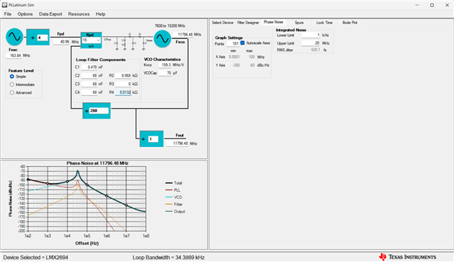
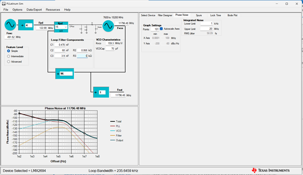
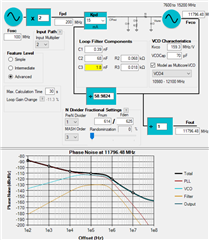
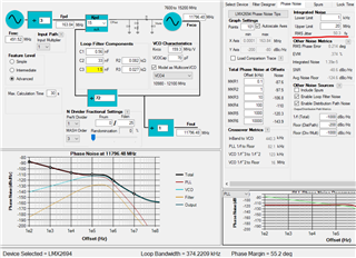
we have one custom design with lmx2694 with it,
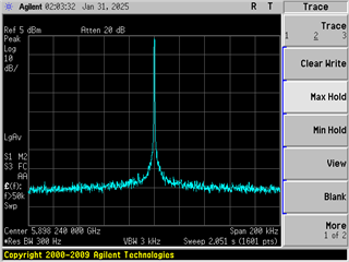
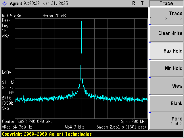
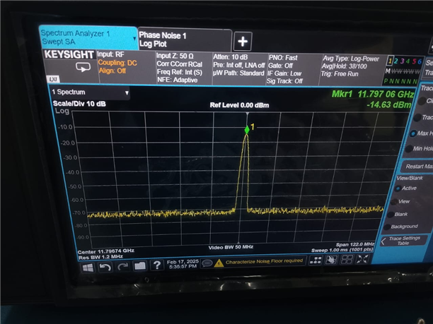
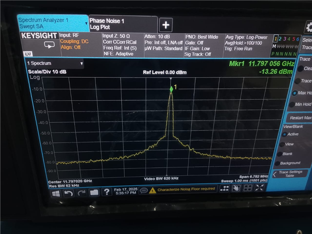
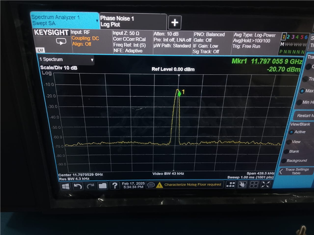
with input clock of lmx2694 is 491.52mhz and output desired clock is 5.898ghz at RFoutB port!
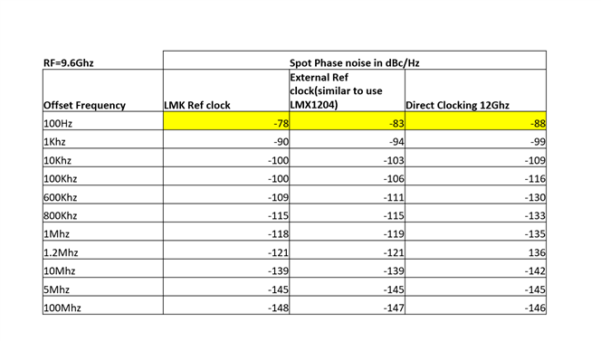
clock is generating @ desired centre frequency but side lobes are added to it, which cant be acceptable in design perspective.
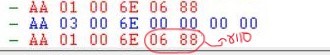
registers used and signal picture are both attached below.
hope this issue solves very soon.
thanks in advance!
R114 0x720000 R113 0x710000 R112 0x700000 R111 0x6F0000 R110 0x6E0000 R109 0x6D0000 R108 0x6C00F1 R107 0x6B0000 R106 0x6A0007 R105 0x694440 R104 0x680000 R103 0x670000 R102 0x660000 R101 0x650000 R100 0x640000 R99 0x630000 R98 0x620000 R97 0x610000 R96 0x600000 R95 0x5F0000 R94 0x5E0000 R93 0x5D0000 R92 0x5C0000 R91 0x5B0000 R90 0x5A0000 R89 0x590000 R88 0x580000 R87 0x570000 R86 0x560000 R85 0x550000 R84 0x540000 R83 0x530000 R82 0x520000 R81 0x510000 R80 0x500000 R79 0x4F0000 R78 0x4E0064 R77 0x4D0000 R76 0x4C000C R75 0x4B0800 R74 0x4A0000 R73 0x49003F R72 0x480001 R71 0x470080 R70 0x46C350 R69 0x450000 R68 0x4403E8 R67 0x430000 R66 0x4201F4 R65 0x410000 R64 0x401388 R63 0x3F0000 R62 0x3E0322 R61 0x3D00A8 R60 0x3C09C4 R59 0x3B0001 R58 0x3A0001 R57 0x390020 R56 0x380000 R55 0x370000 R54 0x360000 R53 0x350000 R52 0x340420 R51 0x330080 R50 0x320000 R49 0x314180 R48 0x300300 R47 0x2F0300 R46 0x2E07FC R45 0x2DC8DF R44 0x2C1F23 R43 0x2B0000 R42 0x2A0000 R41 0x290000 R40 0x280000 R39 0x27DA80 R38 0x26FD51 R37 0x258404 R36 0x240180 R35 0x230004 R34 0x220000 R33 0x211E21 R32 0x200393 R31 0x1F03EC R30 0x1E318C R29 0x1D318C R28 0x1C0488 R27 0x1B0002 R26 0x1A0DB0 R25 0x190624 R24 0x18071A R23 0x17007C R22 0x160001 R21 0x150401 R20 0x14E848 R19 0x1327B7 R18 0x120064 R17 0x11012C R16 0x100080 R15 0x0F064F R14 0x0E1E70 R13 0x0D4000 R12 0x0C5004 R11 0x0B0048 R10 0x0A10D8 R9 0x090604 R8 0x082000 R7 0x0700B2 R6 0x067802 R5 0x0503E8 R4 0x040E43 R3 0x030642 R2 0x020500 R1 0x01080C R0 0x00201C
Hi Vamsi,
this is an integer channel, there will be no spurs so the lobes you are seeing are not spurs from the synthesizer.
Can you confirm it is indeed locked? You can confirm this with the MUXOUT set as Lock Detect output and also reading back register R110 rb_LD_VTUNE.
Can you also measure the reference clock to see if has similar lobes?
I believe the reference clock is a differential clock, how did you connect it to the LMX device?
Hi Noel sir,
First of all. Extremely sorry for late response.
i understood 3 questions from this conversation. ill try to answer all.
1. Does reference clock also have similar side lobes?
-> No, reference signal didnot observed any side lobes.
2. Is reference clock for lmk is differential and how did it connected to lmx?
-> Yes it is differential, it is coming from a ic called lmk04832.
3. is rb_LD_VTUNE locked?
-> Yes it is, checked from reading from MUXOUT (R110[10:9]= 2)(attached picture for reference)
Looking forward for support sir.
thanks:)
Hi Vamsi,
0x0688 means it is unlocked. If it is locked, it should be 0x0488.
How did you connect the clock between LMK04832 and LMX2694?
Hi sir,
My Bad!
Coming Back to the question!
Above mentioned is the path from lmk to afe which is coming from CLKOUT12 p and n. and those are feeding to lmx as below mentioned.
lmk04832 registers are mentioned in code snippet!
thanks sir!
R0 0x000090 R0 0x000010 R2 0x000200 R3 0x000306 R4 0x0004D1 R5 0x000563 R6 0x000670 R12 0x000C51 R13 0x000D04 R256 0x010018 R257 0x01010A R258 0x010210 R259 0x010340 R260 0x010430 R261 0x010500 R262 0x010601 R263 0x010711 R264 0x010806 R265 0x01090A R266 0x010AF0 R267 0x010B40 R268 0x010C30 R269 0x010D00 R270 0x010E01 R271 0x010F13 R272 0x01100C R273 0x01110A R274 0x011290 R275 0x011340 R276 0x011410 R277 0x011500 R278 0x011601 R279 0x011700 R280 0x011808 R281 0x01190A R282 0x011A90 R283 0x011B40 R284 0x011C10 R285 0x011D00 R286 0x011E01 R287 0x011F33 R288 0x012018 R289 0x01210A R290 0x012290 R291 0x012340 R292 0x012430 R293 0x012500 R294 0x012601 R295 0x012711 R296 0x012808 R297 0x01290A R298 0x012A90 R299 0x012B40 R300 0x012C10 R301 0x012D00 R302 0x012E01 R303 0x012F00 R304 0x013006 R305 0x01310A R306 0x013210 R307 0x013340 R308 0x013410 R309 0x013500 R310 0x013601 R311 0x013701 R312 0x013821 R313 0x013900 R314 0x013A0C R315 0x013B00 R316 0x013C00 R317 0x013D08 R318 0x013E03 R319 0x013F00 R320 0x01408F R321 0x014100 R322 0x014200 R323 0x014311 R324 0x014400 R325 0x014500 R326 0x014618 R327 0x01471A R328 0x014802 R329 0x014942 R330 0x014A03 R331 0x014B06 R332 0x014C00 R333 0x014D00 R334 0x014EC0 R335 0x014F7F R336 0x015001 R337 0x015102 R338 0x015200 R339 0x015300 R340 0x015478 R341 0x015500 R342 0x015678 R343 0x015700 R344 0x015896 R345 0x015900 R346 0x015A78 R347 0x015BD4 R348 0x015C20 R349 0x015D00 R350 0x015E1E R351 0x015F0B R352 0x016000 R353 0x016101 R354 0x016244 R355 0x016300 R356 0x016400 R357 0x01650C R358 0x016600 R359 0x016700 R361 0x016958 R362 0x016A20 R363 0x016B00 R366 0x016E13 R371 0x017310 R375 0x017700 R386 0x018200 R387 0x018300 R388 0x018480 R389 0x018500 R392 0x018800 R360 0x01680C R1365 0x055500
Hi sir,
Need to add some more information to the form actually. We actually tried to make the lock up with 25MHz reference clock, and got locked status from r110, but side lobes are still existing. video and registers used are mentioned below.
R114 0x72026F R113 0x710001 R112 0x70012F R111 0x6F001F R110 0x6E0488 R109 0x6D9D7D R108 0x6C00F2 R107 0x6B4001 R106 0x6A0007 R105 0x694440 R104 0x680000 R103 0x670000 R102 0x660000 R101 0x650000 R100 0x640000 R99 0x630000 R98 0x620000 R97 0x610000 R96 0x600000 R95 0x5F0000 R94 0x5E0000 R93 0x5D0000 R92 0x5C0000 R91 0x5B0000 R90 0x5A0000 R89 0x590000 R88 0x580000 R87 0x570000 R86 0x560000 R85 0x550000 R84 0x540000 R83 0x530000 R82 0x520000 R81 0x510000 R80 0x500000 R79 0x4F0000 R78 0x4E0064 R77 0x4D0000 R76 0x4C000C R75 0x4B0800 R74 0x4A0000 R73 0x49003F R72 0x480001 R71 0x470080 R70 0x46C350 R69 0x450000 R68 0x4403E8 R67 0x430000 R66 0x4201F4 R65 0x410000 R64 0x401388 R63 0x3F0000 R62 0x3E0322 R61 0x3D00A8 R60 0x3C09C4 R59 0x3B0001 R58 0x3A8001 R57 0x390020 R56 0x380000 R55 0x370000 R54 0x360000 R53 0x350000 R52 0x340420 R51 0x330080 R50 0x320000 R49 0x314180 R48 0x300300 R47 0x2F0300 R46 0x2E07FC R45 0x2DC8DF R44 0x2C1F23 R43 0x2BDA7F R42 0x2AFD51 R41 0x290000 R40 0x280000 R39 0x27DA80 R38 0x26FD51 R37 0x250404 R36 0x2401D7 R35 0x230004 R34 0x220000 R33 0x211E21 R32 0x200393 R31 0x1F03EC R30 0x1E318C R29 0x1D318C R28 0x1C0488 R27 0x1B0002 R26 0x1A0DB0 R25 0x190624 R24 0x18071A R23 0x17007C R22 0x160001 R21 0x150401 R20 0x14E848 R19 0x1327B7 R18 0x120064 R17 0x11012C R16 0x100080 R15 0x0F064F R14 0x0E1E70 R13 0x0D4000 R12 0x0C5001 R11 0x0B0018 R10 0x0A10D8 R9 0x090604 R8 0x082000 R7 0x0700B2 R6 0x067802 R5 0x0503E8 R4 0x040E43 R3 0x030642 R2 0x020500 R1 0x010808 R0 0x002018
R114 0x72026F R113 0x710001 R112 0x70012F R111 0x6F001F R110 0x6E0488 R109 0x6D9D7D R108 0x6C00F2 R107 0x6B4001 R106 0x6A0007 R105 0x694440 R104 0x680000 R103 0x670000 R102 0x660000 R101 0x650000 R100 0x640000 R99 0x630000 R98 0x620000 R97 0x610000 R96 0x600000 R95 0x5F0000 R94 0x5E0000 R93 0x5D0000 R92 0x5C0000 R91 0x5B0000 R90 0x5A0000 R89 0x590000 R88 0x580000 R87 0x570000 R86 0x560000 R85 0x550000 R84 0x540000 R83 0x530000 R82 0x520000 R81 0x510000 R80 0x500000 R79 0x4F0000 R78 0x4E0064 R77 0x4D0000 R76 0x4C000C R75 0x4B0800 R74 0x4A0000 R73 0x49003F R72 0x480001 R71 0x470080 R70 0x46C350 R69 0x450000 R68 0x4403E8 R67 0x430000 R66 0x4201F4 R65 0x410000 R64 0x401388 R63 0x3F0000 R62 0x3E0322 R61 0x3D00A8 R60 0x3C09C4 R59 0x3B0001 R58 0x3A8001 R57 0x390020 R56 0x380000 R55 0x370000 R54 0x360000 R53 0x350000 R52 0x340420 R51 0x330080 R50 0x320000 R49 0x314180 R48 0x300300 R47 0x2F0300 R46 0x2E07FC R45 0x2DC8DF R44 0x2C1F23 R43 0x2BAD97 R42 0x2A0741 R41 0x290000 R40 0x280000 R39 0x27DA80 R38 0x26FD51 R37 0x250404 R36 0x240060 R35 0x230004 R34 0x220000 R33 0x211E21 R32 0x200393 R31 0x1F03EC R30 0x1E318C R29 0x1D318C R28 0x1C0488 R27 0x1B0002 R26 0x1A0DB0 R25 0x190624 R24 0x18071A R23 0x17007C R22 0x160001 R21 0x150401 R20 0x14E848 R19 0x1327B7 R18 0x120064 R17 0x11012C R16 0x100080 R15 0x0F064F R14 0x0E1E70 R13 0x0D4000 R12 0x0C5001 R11 0x0B0018 R10 0x0A10D8 R9 0x090604 R8 0x082000 R7 0x0700B2 R6 0x067802 R5 0x0503E8 R4 0x040E43 R3 0x030642 R2 0x020500 R1 0x01080A R0 0x002118
Hi sir,
To add on more information to it. we tried different set of clock in reference from lmk to lmx. few clock set lock is establishing. That includes, 24.9925423729 mhz, 92.16 mhz, 163.84 mhz. But our desired ref clock in i.e, 491.52mhz is not establishing. But that is fine , we actually can survive on 163.84mhz clock in where lock is establishing. but as i mentioned earlier sir, in that clock in reference also we are seeing the side lobes.
side lobe delta to main signal picture is mentioned below and r110 read back register also mentioned below.
thanks.
Hi Vamsi,
The EVM experiment shown the spurs are not always appear, I strongly believe there is interference in the environment. The configuration is an integer channel, there is no way to generate a 40kHz spurs. Even if the spurs is generated by the synthesizer, the spurs should stay there all the time. I will take some data tomorrow.
Hi sir,
Any information or solution you add on to the custom board we made with lmk clock as reference to the lmx. where side lobes are always present in that actually. trace max hold picture is attached previously for reference and used registers and also mentioned previously for both lmk and lmx.
Any other information you need, plss feel free to ping. we will make sure all the information is given from our side to get solution for this A.S.A.P sir. We stuck in critical timeline actually.
thanks:)
Hi Vamsi,
Your configuration in the video is an integer channel but your register dump is a fractional channel.
Anyway, I tried both configurations and the result is expected, there is no 40kHz spurs.
below is the max hold plot.
Can you test again with another test equipment?
Hi sir,
we tried with different equipment as well but spurs remained similar. as mentioned below.
need to add some more information to the forum actually.
below is the input clock to the lmx from lmk.
but when we remove the ground connection(from spectrum analyzer) we have seen similar kind of spurs in input clock that is mentioned below.
do you think grounding connection leads to this issue by any chance?
thanks
Hi Vamsi,
Looks to me you are using some kind of probe to measure the signal. Is it possible to connect the output of the synthesizer directly to the test equipment?
Your input clock spurs is about 20dBc, which is too high to be believable.
The spurs in the first plot looks like your PLL loop filter phase margin is too small, what is your loop filter bandwidth and phase margin?
Hi sir,
In our custom board we dont have provision to directly connect the output of lmk04832 to test equipment. But we have the provision of connecting the output of lmx2694 to the test equipment. those snips are already attached in the forum.
and regarding phase margin and loop filter bandwidth of lmx, may i know where to check that, went through tics pro, but couldnt found that actually.
thanks.
Hi Vamsi,
the 5.898GHz signal is -50dBm, this is too small if the LMX2694 output is directly connected to the test equipment.
PLL is a close-loop system, loop bandwidth and phase margin represent the characteristic of the loop.
What is your loop filter design, phase detector frequency and charge pump current? we need these information to calculate loop bandwidth and phase margin.
Hi sir,
Above is the picture of lmx evm output with the same registers and clock frequency, this power level also similar, this has nothing to do with probing sir, may be some setting issue in this equipment, previous equipment photos power level seems to be fine. But the main concern is not the power level but the side lobes are still existing when tested on different equipment as well sir.
We will update you with phase margin and loop filter bw, using platinum sim tool.
Thanks!
Hi Vamsi,
below is the plot I attached previously, output power should be around 5dBm.
Hi sir,
Freq offset(SSB)(ddc/hz)
|
AFE with lmk-04832
|
AFE with lmx-2694
|
TI REF data (AFE WITH LMX)(@9.6gig centre)
|
100Hz
|
-72.49
|
-76.10
|
-88
|
1Khz
|
-92.11
|
-94.08
|
-99
|
10khz
|
-101.45
|
-102.72
|
-109
|
100Khz
|
-101.20
|
-100.91
|
-116
|
1mhz
|
-120.91
|
-121.76
|
-135
|
Hi Vamsi,
With LMX2694 eval board default configuration and a good reference clock, the sim result has better phase noise than your configuration. This is probably due to lower fpd in your configuration.
Default eval board configuration.
You can make fpd higher, for example,
How does the 491.52MHz clock look like? This clock also affect LMX2694 output phase noise.