This thread has been locked.

If you have a related question, please click the "Ask a related question" button in the top right corner. The newly created question will be automatically linked to this question.

LMX1204: The reason for LOGICCLKOUT ringing

Part Number: LMX1204

Tool/software:

Dear Specialists,

My customer is evaluating LMX1204 and has questions.

I would be grateful if you could advise.

---Question

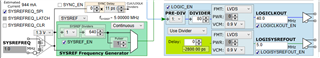
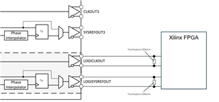
As shown in the attached configuration, the LOGICLKOUT of the LMX1204 is connected to the FPGA.

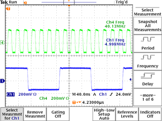
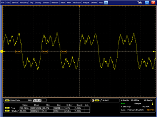
When observing the LOGICLKOUT waveform at the FPGA end, large ringing was observed.

-Set the output format of both LOGICLKOUT and LOGISYSREFOUT to LVDS.

-Connected to FPGA by DC coupling (direct connection).

-Install a 100Ω termination resistor on the FPGA side (receiving end).

When observing the LOGICLKOUT waveform at the FPGA end, ringing like the one shown below occurs.

Q1:

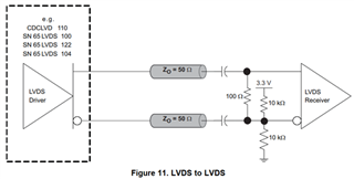
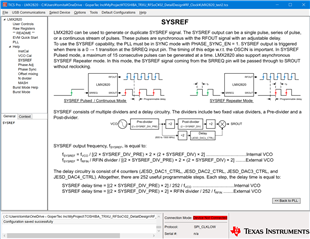
According to the circuit diagram in the LMX1204EVM User's Guide

The output is output to the SMA connector by AC coupling (0.1uF).

Is AC coupling necessary for LVDS output?

※Does this mean DC coupling cannot be used?

Q2:
If DC coupling is possible, is it sufficient to only use 100 Ω termination on the receiving side as shown in the attached diagram?

Q3:
As far as I understand, the only register settings related to LVDS output are the output format and VCM settings.

Are there any other settings that need to be set?

I have attached the configuration file to this email, so if there are any errors in the settings, I would appreciate it if you could let me know.

Q4:
If there are no problems with the configuration, connections, or settings, what do you think could be the cause of the severe ringing as shown in the attached diagram?

However, when I modified this configuration to use LVPECL (AC coupling), the ringing did not occur and the clock waveform was fine, so I do not think there is a problem with the wiring pattern on the printed circuit board.

ーーー

I appreciate your great help in advance.

Best regards,

Shinichi

  • Hi Shinichi-san,

    I will be able to answer your question tomorrow.

    Thanks,

    Michael

  • Hi again Shinichi-san,

    Q1: The CLK outputs of the LMX1204 should not be DC coupled. The outputs of the LMX1204EVM are AC coupled due to the fact that most devices operating at RF frequencies are very sensitive and require the DC bias to be removed. AC coupling the LOGICLKOUT signal should be fine, so long as the frequency remains below the RF range. However, please try my suggestion in Q4 before removing the caps.  

    Q2: The termination looks good and should be fine.

    Q3: I cannot see your configuration. Would you care to re-attach it so I may look through it?

    Q4: Considering that you got LVPECL to work with the AC coupling caps, I believe the ringing may be caused by inappropriate output termination. Based on the picture of your scope, it looked like you only input one signal. Would it be possible for you to input both the P and N pins of LOGICLKOUT to the scope and create a Math channel that subtracts one from the other? Otherwise, one of the outputs will have a 50 Ohm termination to GND, and the other will not, which could cause such problems in a closed-circuit driving format like LVDS.

    One thing of note is that if you do decide to DC couple the LOGICLKOUT outputs, you will need to connect an emitter resistor to GND in order for LVPECL to work (see page 39 of the datasheet, in the LOGICLKOUT_FMT section). 

    Thanks,

    Michael

  • Hi Michael,

    Thank you for your reply.

    I attached the file.

    Could you please see and advise?

    Regarding Q3, could you please see attached file.

    Q3:
    As far as I understand, the only register settings related to LVDS output are the output format and VCM settings.

    Are there any other settings that need to be set?

    I have attached the configuration file to this email, so if there are any errors in the settings, I would appreciate it if you could let me know.

    [SETUP]
    ADDRESS=888
    CLOCK=8
    DATA=4
    LE=2
    PART=LMX1204
    IFACE=SPI
    ADDRESS_I2C=0x0
    
    [PINS]
    PINNAME00=CE
    LOCATION00=7
    PINVALUE00=True
    
    [MODES]
    NAME00=R90
    VALUE00=5898240
    NAME01=R86
    VALUE01=5636100
    NAME02=R79
    VALUE02=5177349
    NAME03=R76
    VALUE03=4980736
    NAME04=R75
    VALUE04=4915203
    NAME05=R72
    VALUE05=4718593
    NAME06=R67
    VALUE06=4411851
    NAME07=R65
    VALUE07=4285456
    NAME08=R34
    VALUE08=2228229
    NAME09=R33
    VALUE09=2188902
    NAME10=R29
    VALUE10=1902079
    NAME11=R28
    VALUE11=1837576
    NAME12=R25
    VALUE12=1638937
    NAME13=R24
    VALUE13=1572865
    NAME14=R23
    VALUE14=1564736
    NAME15=R22
    VALUE15=1442936
    NAME16=R21
    VALUE16=1380088
    NAME17=R20
    VALUE17=1314552
    NAME18=R19
    VALUE18=1249016
    NAME19=R18
    VALUE19=1183480
    NAME20=R17
    VALUE20=1114228
    NAME21=R16
    VALUE21=1052800
    NAME22=R15
    VALUE22=985984
    NAME23=R14
    VALUE23=917506
    NAME24=R13
    VALUE24=851970
    NAME25=R12
    VALUE25=786432
    NAME26=R11
    VALUE26=720896
    NAME27=R9
    VALUE27=606216
    NAME28=R8
    VALUE28=524592
    NAME29=R7
    VALUE29=489473
    NAME30=R6
    VALUE30=444708
    NAME31=R5
    VALUE31=346422
    NAME32=R4
    VALUE32=276223
    NAME33=R3
    VALUE33=262022
    NAME34=R2
    VALUE34=131203
    NAME35=R0
    VALUE35=0
    
    [FLEX]
    CLKIN_FREQ=3200.0
    CLKOUT0_FREQ=3200.0
    CLKOUT1_FREQ=3200.0
    CLKOUT2_FREQ=3200.0
    CLKOUT3_FREQ=3200.0
    LOGICLKOUT_FREQ=100.0
    LOGISYSREFOUT_FREQ=6.25
    SYSREFOUT0_FREQ=6.25
    SYSREFOUT1_FREQ=6.25
    SYSREFOUT2_FREQ=6.25
    SYSREFOUT3_FREQ=6.25
    SYSREFREQ_FREQ=6.25
    btnMULT_CAL=Calibrate Multiplier
    btnRB_LD=Read Lock Detect
    btnREAD_SYSWIN=Read SYSWIN Position
    btnREAD_TEMP=Read
    spnSYSDLY0=6
    spnSYSDLY1=0
    spnSYSDLY2=0
    spnSYSDLY3=0
    spnSYSDLY4=1
    stCLKPOS=0
    stCLKPWR0=+6.1 dBm
    stCLKPWR1=+6.1 dBm
    stCLKPWR2=+6.1 dBm
    stCLKPWR3=+6.1 dBm
    stCURRENT=807 mA
    stDELAY_RANGE=[-1250.00, 1245.08] ps
    stDELAY_STEPSIZE=4.92 ps
    stDLY0=-1458.66 ps
    stDLY1=-1458.66 ps
    stDLY2=-1458.66 ps
    stDLY3=-1458.66 ps
    stDLY4=-1633.66 ps
    stFACTOR=
    stFINTERPOLATOR=400.00000 MHz
    stFSMCLK=Disabled
    stFSYSREF=6.25000 MHz
    stPWR0=0.48 Vpp
    stPWR1=0.44 Vpp
    stPWR2=-- Vpp
    stPWR3=-- Vpp
    stTJ=-- °C
    stVCM0=1.00 V
    stVCM1=1.67 V
    stVCM2=-- V
    stVCM3=-- V
    AUTOSET_IQ=1
    AUTOSET_LOGICLK_DIV_PRE=1
    AUTOSET_SMCLK=1
    AUTOSET_SYSREFREQ_DELAY_STEPSIZE=1
    AUTOSET_SYSREFREQ_DELAY_STEP_SCALE=0
    AUTOSET_SYSREF_DELAY_DIV=1
    AUTOSET_SYSREF_DIV_PRE=1
    WINDOW_STATUS=ERROR: Set CLKPOS_CAPTURE_EN or results will be invalid
    btnREAD_WINDOW=Read CLKPOS
    tcCLKDLY0=125.00 ps
    tcCLKDLY1=125.00 ps
    tcCLKDLY2=125.00 ps
    tcCLKDLY3=125.00 ps
    tcCLKDLY4=300.00 ps
    tcCLKSYSDLY0=-1458.66 ps
    tcCLKSYSDLY1=-1458.66 ps
    tcCLKSYSDLY2=-1458.66 ps
    tcCLKSYSDLY3=-1458.66 ps
    tcCLKSYSDLY4=-1633.66 ps
    tcCurrent_CLKout=265 mA
    tcCurrent_Core=294 mA
    tcCurrent_LOGICLKout=12 mA
    tcCurrent_LOGISYSREFout=77 mA
    tcCurrent_SYSREFGen=80 mA
    tcCurrent_SYSREFout=79 mA
    tcCurrent_Total=807 mA
    tcSYSDLY0=-1333.66 ps
    tcSYSDLY1=-1333.66 ps
    tcSYSDLY2=-1333.66 ps
    tcSYSDLY3=-1333.66 ps
    tcSYSDLY4=-1333.66 ps
    tcStep0=-271
    tcStep1=-271
    tcStep2=-271
    tcStep3=-271
    tcStep4=-271


    I appreciate your great help and cooperation.

    Best regards,

    Shinichi

  • Shinichi-san,

    I will take a look over your register configurations tomorrow. In the meantime, can you confirm whether the signal measurement you took was single-ended? Taking a single-ended measurement on one of the outputs of an LVDS output driver would cause the ringing you saw. I believe if you connected to both outputs and channeled it through a balun, the signal would look as expected.

    Thanks,

    Michael

  • Hi Michael,

    I could obtain the feedback from the customer.

    Could you please advise?

    ----

    Q1: The CLK outputs of the LMX1204 should not be DC coupled. The outputs of the LMX1204EVM are AC coupled due to the fact that most devices operating at RF frequencies are very sensitive and require the DC bias to be removed. AC coupling the LOGICLKOUT signal should be fine, so long as the frequency remains below the RF range. However, please try my suggestion in Q4 before removing the caps.  

    I understand that AC coupling is recommended.
    In the case of AC coupling, I think an external circuit is necessary to match the VCM of the receiving side (FPGA, I/O standard is LVDS).
    Is the receiving side setting shown in the diagram below OK?

    #Quoted from TI document: SCAA059C "AC-Coupling Between Differential LVPECL, LVDS, HSTL, and CML"

    Q2: The termination looks good and should be fine.

    You mentioned that there is no problem with the termination, but the waveform I sent you the other day with a large ringing was obtained with this connection (LVDS output).

    The measurement was taken with a differential probe at both ends of the 100Ω termination, so I do not think that the ringing is caused by an imbalance in the +/- signal.

    Q3: I cannot see your configuration. Would you care to re-attach it so I may look through it?

    Could you please share when you confirm.

    Q4: Considering that you got LVPECL to work with the AC coupling caps, I believe the ringing may be caused by inappropriate output termination. Based on the picture of your scope, it looked like you only input one signal. Would it be possible for you to input both the P and N pins of LOGICLKOUT to the scope and create a Math channel that subtracts one from the other? Otherwise, one of the outputs will have a 50 Ohm termination to GND, and the other will not, which could cause such problems in a closed-circuit driving format like LVDS.

    I used a differential probe for the measurement. Is it inappropriate to use a differential probe?

    One thing of note is that if you do decide to DC couple the LOGICLKOUT outputs, you will need to connect an emitter resistor to GND in order for LVPECL to work (see page 39 of the datasheet, in the LOGICLKOUT_FMT section). 

    I would like to find a solution with LVDS output.

    Could you please advise?

    ---

    I appreciate your great help and cooperation.

    Best regards,

    Shinichi

  • Hi Shinichi-san,

    I will get to your question soon.

    Thanks,

    Michael

  • Hi Shinichi-san,

    Sorry for the multiple responses, we have to reply for an internal metric. 

    I accidentally mistyped earlier. It should be okay to DC couple your LOGICLK outputs so long as the frequency remains below the RF range. The figure you have attached should be fine. I am actually curious to see how the output will be changed if the AC coupling caps are removed. Could you try that and show me the output?

    Can you send me the full schematic and re-send your configuration file as a .tcs file? I cannot use the file you sent me. 

    Thanks,

    Michael

  • Hi again Shinichi-san,

    I took your setup into lab and I believe I have recreated your issue! I was seeing the ringing that you saw when I set the pre-divide value to a value greater than 1 (i.e. 2 or 4) and bypassed the dividers. 

    The pictures below document what the output of my LOGICLK looked like and at what settings.

    In the above image, I have configured the LOGICLK output dividers to output a frequency of 160 MHz with a pre-divide value of 1. When I change that value to 2, I get the scope shot below:

    So far, I had behavior as anticipated. However, when I changed the setting from "Use Divider" to "Bypass Divider" with the pre-divide value of 2, I saw the output below:

    When I changed the pre-divide value to 4, the ringing got even worse:

    When I changed the pre-divide value to 1, the ringing was reduced:

    I believe that in your setup, the ringing can be reduced by using the dividers (if you are not already) and by setting the pre-divider to 1, and using a larger divider value.

    Thanks,

    Michael

  • Hi Michael,

    Thank you for your reply.

    I understand pre-divider should be 1 and increase divider value.

    I'll share this information with the customer.

    I appreciate your great help and cooperation.

    Best regards,

    Shinichi

  • Hi Michael,

    I sent your suggestion, but Phenomenon was not improved.

    Could you please see attached file and advise?

    result0218.pdf

    I appreciate your great help and cooperation.

    Best regards,

    Shinichi

  • Hi Shinichi-san,

    I am going to be out of office on vacation for the next 10 days. I will loop in another AE to assist you. 

    Thanks,

    Michael

  • Hi Inoue-san,

    Your configuration uses "User Divider", there should be no ringing issue.

    Below is my test data.

    Configuration file.

    2867.1204e2e.tcs

  • Hi Noel,

    Thank you for your reply.

    I understand you cannot confirm output ringing with the customer's setting.

    I'll share with the customer.

    I have a question, could you please advise.

    Did you check with LMX1204EVM?

    I appreciate your great help and cooperation.

    Best regards,

    Shinichi

  • Hi Inoue-san,

    My data was taken from the LMX1204EVM.

  • Hi Noel,

    Thank you for your reply and I'm sorry for late reply.

    The customer understood that there may be a problem with the pattern layout.

    However, due to lack of time to fix, they decided to use LVPECL or CML.

    I appreciate your great help and cooperation.

    Best regards,

    Shinichi