This thread has been locked.

If you have a related question, please click the "Ask a related question" button in the top right corner. The newly created question will be automatically linked to this question.

LMK00804B: Seeing noise injected on input when LVCMOS input is sleected

Part Number: LMK00804B
Other Parts Discussed in Thread: LMK1C1104, LMK00304, LMK00334, LMK00804

Tool/software:

I am seeing an issue where noise is being injected on an input to the part, as well as the output becomes unusable/unstable.

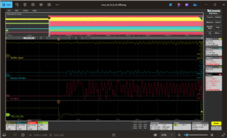
With a 1Hz (1 PPS) input on both the LVCMOS and the DIFF input set up as a CMOS input, I see noise on all inputs and the output when the CLK_SEL is changed from a 1 to a 0.

When it is at a 1, both inputs look fine and the output follows the selected input.  It is when I change the CLK_SEL to be a 0 that I see the issue,

What should I be looking towards to help determine why I am seeing this error.  I also see this issue if I don't drive the LVCMOS input with any signal.

In attached pictures.  Buffer input = LVCMOS input)    Resistor Divider is the P half of the diff input.  ZL_INPUT is the output of the LMK008804   PPS_CLK_SEL is the select input.

  • Hello James, 
    What is the ref clk in this case? 
    I find this very odd - could you also share your schematic? 

    Best regards, 

    Vicente 

  • Hi Vicente,

    Any insight or observation regarding this issue?

    Thanks

    -Jim D.

  • Hi Vicente,

    Gentle reminder.

    Also, I have some other engineers that would like to follow this case as well.

    Is it possible to add people to this case.

    Thanks

    -Jim D.

  • Hi Jim, 

    Sorry for the delayed response here, Vicente is out of office and the rest of the team didn't see there was a new reply on this thread. 

    It looks like the rise time on the input is around 2.5us. This would give a slew rate of around 3.3V / 2.5 us = 0.00132 V/ns which is well below the recommended value (see section 10.6.3 of the LMK00804B datasheet for input slew rate considerations) and can cause chattering on the output. 

    If possible, you could try increasing the input slew rate. Another option is to use LMK1C1104 which can tolerate much lower input slew rates and might be more suitable for a 1pps application. 

    Regards, 

    Connor 

  • Hi Connor,

    When I zoomed in on the leading edge I was getting about a 20ns risetime on the LVCMOS input and a 15ns risetime on the CLKp input.  I did try an experiment to improve the risetime of the LVCMOS input and got it down to about 10ns.  This was done with an easy change of a series resistor.  To improve it even more will take a little rework of the card.  But I was actually starting to head in that direction.

    Do you believe that the improved risetime would alleviate the problem an improve the signal?  Does it make sense that when I select the 15ns rt of diff input the signal looks fine, but when I select 20ns rt of the lvcmos input I get all that chatter.  I was thinking that by chatter the datasheet refers to was more phase-noise versus unstable output.

    I am not able to use the 1104 as I need to be able to select between the two clocks.  In reality I need to select between 3 clocks.  Could you recommend a device that can select between 3 lvcmos inputs and drive 3 outputs.

    Thanks

    -Jim D.

  • Thanks for the clarification, if the rise time is actually in the 10-20ns range then the input slew rate may not be the problem. Can you share a schematic of your setup?

    Unfortunately our 3-input buffer options are somewhat limited. We have LMK00304/LMK00334 which could work, but the OSCin pin needs to be AC-coupled which may be an issue at 1Hz. Do you need LVCMOS outputs, or would a differential output format work? 

    Regards, 

    Connor 

  • How do I get the schematics to you?

    I see I can drop them into the chat, but not sure if other people who are browsing thru the forum would be able to download them

  • You can attach the schematic images here, but other people reading through the forum would be able to see the attachments. If you prefer to keep them private we can move this discussion to an email thread. 

    I'm mainly interested in the input/output terminations of the buffer, if you could send a snippet of just that portion that would work as well. 

    Regards, 

    Connor 

  • Scope trace of CLK input to LMK00804

    I have an initial mistake in the design that I will be correcting on a new layout and has been corrected on the card under test.  The differential CLK input comes from a FET switch where only one of the inputs has the pullup/pulldown on it.  For the card under test I have moved them to be on the CLK pin of the LMK00804 itself.  (100ohm each for PU/PD.  Will be changing to a lower value to get the diff signal to be < 1.3V).

    LMK00804 under test : U5001

                    LVCMOS input : OCB_CB_GPS_PPS from a backplane connector which is driven by this same part on the other card.

                    CLK input : PPS_MUX_OUT from a FET mux (U5003)

                                    The FET MUX inputs are

                                                    TOD_PPS from a differential receiver that is attached to a RJ45 connector

                                                    GPS_1HZ_SYNCIN from an input buffer that is connected to a DIN connector.

                                                                    This signal has the pullup/down resistors that have been moved to the LMK00804 CLK pin.

    Schematic snippets

  • Hi Jim, 

    Unfortunately I'm not able to open the attachments on your last reply. Can you try sending them again? If that still doesn't work you can start an email thread with me at c-lewis3@ti.com

    Regards, 

    Connor 

  • Hi connor,

    I created a 2 page PDF and attached it.here.  If you still can't see it we can do this via email as you suggested.

    Thanks

    -Jim D.


    e2e_ti_lmk00804b_sch_shots.pdf

  • Hi Jim, 

    Thanks for sending over the new file, I'm able to open it on my end. A few clarification questions: 

    1. Does the "OCB_CB_GPS_PPS" net have any other series components, terminations, etc. on the driver side? Or is it just directly connected to the receiving LMK00804B? VOL = 0.9V and VOH = 2.35V isn't what I'd expect from a LVCMOS driver but the waveform looks pretty clean. 

    2. I see you mentioned that you're successfully using another LMK00804B to drive the 1Hz signal to the LVCMOS input of the receiving LMK00804B (shown on the schematic you sent over). Is there any difference in how they're configured? How long is the total routing between them? 

    I'm not seeing any obvious issues that could explain this behavior. Based on the rest of the system, is there any way that pulling "GPS_PPS_CLK_SEL" low could somehow introduce noise to "OCB_CB_GPS_PPS"? I also wonder if adding a small load (maybe 5-10pF) to the LVCMOS input would help filter out some of this noise, although that's not addressing the root cause of the issue. 

    Regards, 

    Connor 

  • Hi Connor,

    1) There is a series resistor on the output of the other driver.  It is currently 48ohms, on a test card I changed it to 0 ohms to get the faster edge, but that gets alot of overshoot (as expected).  I need to go back and try some other values (maybe 10 is the lucky number).  The signal originates from U5001 pin 14, so the same LMK00804s between the cards are connected together.

    2) there is a lot of etch between the two.  There is 29 inches driver to midplane, thru about 1.5 inches on the midplane, then back into the card receiving it with about 29 more inches of net.

    I'm looking into trying to sharpen the rise time to the lmk00804 inputs.

    Thanks

    -Jim D.

  • Forgot to mention that the waveform shown is the CLKp input of the differential par, not the LVCMOS input.  I will get a scope shot of that and send once I change to a different series term value.

  • Hi Connor,

    Getting a chance to swing back to this issue.  Spoke with an SI eng here and he points out that the output is going unstable the instant I change the CLK_SEL input to the part.  The inputs are stable at the point at which the CLK_SEL line is changed.  He doesn't believe this is a slew rate issue with an input clock.  Can you investigate as to why just changing the CLK_SEL would cause instability on the output.  And why only when it changes from 1 to 0.  When it changes back to a 1 the output becomes stable again.  The last scope shot of the initial 4 shows this.  Also attached some shots with a better sample rate (800ps/pt).  I will see about adding 5pF to the LVCMOS input, but the signal is quite before the CLK_SEL changes.  I'll also se about getting some scope shots with better grounds to the probes.

    Thanks

    -Jim D.

  • Hi Jim, 

    I'll take another look at this and see if I can replicate the same type of behavior on an EVM in our lab, hopefully that will help with finding the root cause. I should be able to get back to you with some results by the end of this week. 

    Regards, 

    Connor 

  • Hi Connor,

    I also tried another experiment where I removed the card from the chassis and powered it up on a bench.  So at this point there really is nothing driving the LVCMOS input to the part.  The part is also not driving anything else except the etch on the card.  In the past I tried removing the card sourcing that input, but left the DUT within the chassis.  For the standalone test I did not see the output misbehave as I did when it was in a system.  But, I am also able to have a better ground on my signal to the scope since I don't need to rely on a wire coming out for ground.  I just got access to a cut out chassis so will try putting the card back and do the better probing in that.  Will also try and add the 5pF cap as you suggested earlier.

    Thanks

    -Jim D.

  • Hi Connor,

    Do you think a large undershoot on the CLK_SEL line could cause this issue?  It looks like I am seeing an undershoot of about -1.8V on the signal.  And it is about this time that the output starts to ring.  Also did an experiment with nothing coming into the LVCMOS input and zoomed in when the CLKSEL changed to 0.  I see ringing on the output at this point, but it settles down to 0 since there is nothing on the input.  Unfortunately, I don't have a series resistor on this signal.  Will see if I can find a diode to put on the CLK_SEL to at least limit its undervoltage better.

  • Hi Jim, 

    I had a chance to try this out on an EVM, and it does seem like an undershoot on CLK_SEL causes some oscillations/glitches on the output. Based on my testing it seems like the threshold is somewhere around -0.7V before this issue comes up. I also see the same oscillation behavior whether or not there is an active input on LVCMOS_CLK. 

    Let me know if you're  able to remove this undershoot on your board, and hopefully this resolves your issue. 

    Regards, 

    Connor