This thread has been locked.

If you have a related question, please click the "Ask a related question" button in the top right corner. The newly created question will be automatically linked to this question.

LMK00301: Clock impedance matching circuit

Part Number: LMK00301


Tool/software:

Dear Experts,

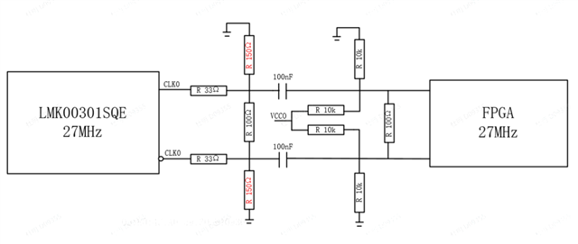
The design schematic diagram is as follows.The design schematic diagram is as follows. Our current FPGA design requirements are: differential input voltage range of 100mV~600mV, common mode input voltage range of 300mV~1125mV, and single ended input voltage overshoot range of -200mV-1200mV. We would like to inquire about the design of clock impedance matching circuit and hope to receive answers. Thank you~
1. Do we need a 150 Ω resistor to ground the AC coupling capacitor?
2. When laying out a single PCB, is it necessary to place the matching circuits of the sending and receiving ends close to the ports respectively? Should AC coupling capacitors also be placed near the transmitting end?

  • Hi Colin, 

    Are you planning on using LVDS or LVPECL for the output of the LMK00301? LVDS might simplify your termination scheme since the swing will be within your spec with a single 100 Ohm differential termination. For LVPECL, the 150 Ohm to GND resistors are required before the AC coupling capacitors to bias the emitter follower stage of the driver. 

    The location of the AC coupling capacitors isn't too critical, but if the trace length between the LMK00301 and FPGA is long then I would put them closer to the driver. The 100 Ohm termination should be placed as close as possible to the FPGA inputs to minimize reflections. 

    Let me know if you have any other questions. 

    Regards, 

    Connor