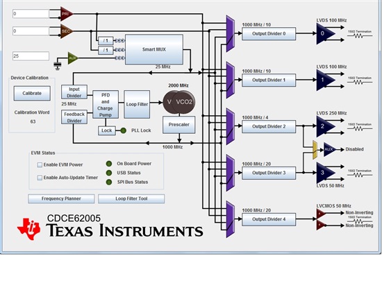
This thread has been locked.

If you have a related question, please click the "Ask a related question" button in the top right corner. The newly created question will be automatically linked to this question.

CDCE62005 registers' value

Other Parts Discussed in Thread: CDCE62005, MSP430F5418A

Hi,

I used the CDCE62005 Controller GUI v1.4.4" generate a register value. I only used an auxilary input crystal of 25MHz to get two 100MHz, one 250MHz and two 50MHz output

respectively. But I don't quite sure about the value I got from the GUI. Can you help me with these values? And how to configue the loop filter?

And the registers' value are as follows:

0 eb060330
1 eb060331
2 eb840302
3 eb0e0303
4 10e03f4
5 10007a55
6 6bff83e6
7 fdfffff7
8 fffffff8

PORTS
0 bf
1 ffffffff
2 ffffffff
3 ffffffff

INPUTS
PRI 0
SEC 0
AUX 25

EXTERNAL COMPONENTS
C4 1
R4 1
C5 1

  • It's still me

    I have another question:

    What does the PORTS in the configure file mean?

    for example,

    PORTS
    0 bf
    1 ffffffff
    2 ffffffff
    3 ffffffff

    Thank you

    Nick

  • Hi Nick,

    thank you for the interest in our device. I checked your register setting and I found out that you are using the external loop filter, which usually is not strickly needed for XTAL input case. I defined my register setting in order to get the same output frequencies and the lock condition as well. Please find them attached.

    In order to get the lock condition I had to tune the loop filter. On the GUI you can use the Loop Filter Tool. Two parameters are important: the Loop Bandwidth and the Phase Margin. In case of XTAL input you can set a wide loopbandwidth. The Phase Margin should be in the range 60 to 70 degree. You can change these parameter by tuning C1, R2,C2, R3 and C3 values. You will see a direct impact on the output jitter performance.

    If you need further detail, please do not hesitate to contact us.

    Best regards,

    Leandro

    REGISTERS
    0 eb060330
    1 eb060331
    2 eb840302
    3 eb0e0303
    4 10e03f4
    5 10007b15
    6 33ff83e6
    7 fdfffff7
    8 800098b8

    PORTS
    0 fd
    1 ff
    2 df
    3 f9

    INPUTS
    PRI 0
    SEC 0
    AUX 25

    EXTERNAL COMPONENTS
    C4 1
    R4 1
    C5 1

  • Hi,Leandro

    Thank you for your detailed reply.

    I still have some problems with these registers. First, you mean I need to configure the internal loop filter to get right output frequency. But I don't quite sure how to

    configure it. And what values of C1, R2,C2, R3 and C3 do I need?

    What's more, what does the the following PORTS parameters mean?

    PORTS
    0 fd
    1 ff
    2 df
    3 f9

    Thank you

    Nick

  • Hi Nick,

    you need to configure the internal loop filter to get the lock condition, after you get the right output frequencies by using the Frequency Planner. The values of C1, R2, C2, R3 and C3 depend on the required loop bandwidth. For an XTAL input case we usually suggest a loop bandwidth in the range 100k-1MHz. I set a Loop Badnwidth of 460kHz and Phase Margin of 62 degree. In this case: C1=11.5p, R2=9k, C2=461p, R3=5k and C3=8p. After pushing the Calibrate button, the Lock condition was achieved.

    I am still checking what PORTS means. I guess it is somehow related to the programming interface.I will come back to you about this topic as soon as I have better info.

    I hope this will help you.

    Best regards,

    Leandro

  • Hi Leandro,

    Thanks a lot for your info. I have one more question, which is by reading the datasheet of CDCE62005, all registers have reserved bits. Some bits say they must be set to 0

    and others say they must be set to 1. What do these  reserved bits mean? Do they have some real meaning? And do I have to do as what the datasheet says?

    Thanks

    Best regards

    Nick

  • Hi Nick,

    the reserved bits are either used by the state engine of the device or for internal test purpose.

    If you use the GUI to generate the register setting for your application, you will realize that the content of the reversed bits matches with the indication on the datasheet. You should not modify them otherwise there will be an impact on the device functionality.

    BTW, in which context/application are you using the CDCE62005?

    Thanks and best regards,

    Leandro

  • Hi Leandro,

    You mean I should strictly follow what the datasheet says about the reserved bits. And do not change the value if the corresponding bit should be set to 0 or 1.

    We use CDCE62005 to generate clock for DSP,FPGA and CPLD. And MSP430F5418A control CDCE62005 to do the above thing.

    Thanks and best regards,

    Nick

  • Hi Nick,

    yes you should strictly follow what the datasheet says about reserved bit. BTW, I want to be sure you are using the latest datasheet version. Please find it in attachment.

    best regards,

    Leandro

    cdce62005[1].pdf
  • Hi Leandro,

    Thank you very much. If I have some other question, I hope you can help me. I really appreciate your help.

    Thanks

    Best regards,

    Nick

  • Hi Leandro,

    I'm sorry to bother you again. I encounter another question when using CDCE62005:

    There are 10 bits which is marked as read only int the 8th register of CDCE62005. At start up, I write all the registers to CDCE62005. If I write the read only bits, is there an

    impact on the device? If there is, what should I do about those read only bits? To ignore them?

    Best regards,

    Thank you

    Nick

  • Hi Nick,

    the read-only bits on the register 8th can not be written. They can just be used to check what the device status is. Therefore if you write them, there should not be any impact on the device.

    Best regards,

    Leandro