Part Number: LMK1D2108
Tool/software:
I just designed and put together a PCB with the schematic attached in pdf. It is driven by by microchip's DSC1103CI2-200.0000 (200MHz), and powered by TI's TPS70933DBVR.
I was hoping the the circuit would work in one shot (so naive of me).
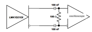
The problem is I see nothing at the SMA output pads, with or without 50 ohm termination. (With 50 ohm termination, I just connect a 100 ohm between P and N clk outputs and connect signals to an oscilloscope (Zin=1Mohm) via BNC.)
My observations:
(0) I see absolutely no oscillations at the buffer's outputs, even the noise has no components close to 200MHz
(1) The DC components of the clk outputs seems random. For some pairs, one pad is at DC 0.8V (P), other at DC 1.8V (N), other pads are pinned at 0.9V (both P and N).
(2) The whole chip draws about 20-30mA (datasheet says ~50-100mA)
(3) Microchip's oscillator LVDS output outputs a correct sine-wave, about 0.5 V pk-pk for clk-P. So the input is working fine
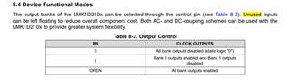
Is the chip dead? Am I not terminating the clk outputs properly? Is the EN pin not supposed to be at 3.3V (inverted logic)?
Here's the 3d model of the PCB for a quick review, if that helps. It took me an hour to design, so I feel safe to attach it here.