


Hi,
There is very little description on the function of S0 pin in the datasheet, and the only I found is that S0 controls whether output is three state in Fig.6 and Table-4.
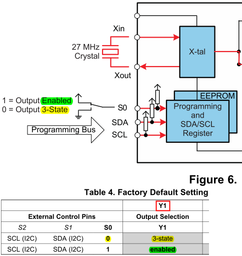
However, Table-4 only listed Y1, not Y2 and Y3. So does S0 control Y1,Y2 and Y3's Enable/3-state at the same time?
And if I want Y1, Y2 and Y3 to be enabled at all time, should I tie S0 to [pin 3, VDD] directly, or via a resistor? If a resistor is needed, what should its resistance be?
Additionally, controlling whether output is 3-state is a very simple operation; and since CDCE913 already has I2C ports equipped, it can easily be designed to let an I2C register bit control Y1, Y2, Y3's output Enable/3-state. So why there still bothers to a separate S0 pin at the cost of both increased footprint and added connections on the external circuit?
Tim

