A related question is a question created from another question. When the related question is created, it will be automatically linked to the original question.
If you have a related question, please click the "Ask a related question" button in the top right corner. The newly created question will be automatically linked to this question.
-> since our output only generates a single set of refclk, we only pull one OE.
CLK_SEL will be determined as High (H) or Low (L) through our internal GPIO to allow CLKIN0/1 to output to the final output. (Please correct me if there are any errors.)
What is the purpose of the capacitor to GND?
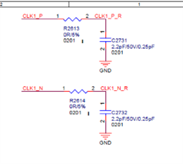
→ As shown in LMKDB1202_Application_Circuit.pdf.
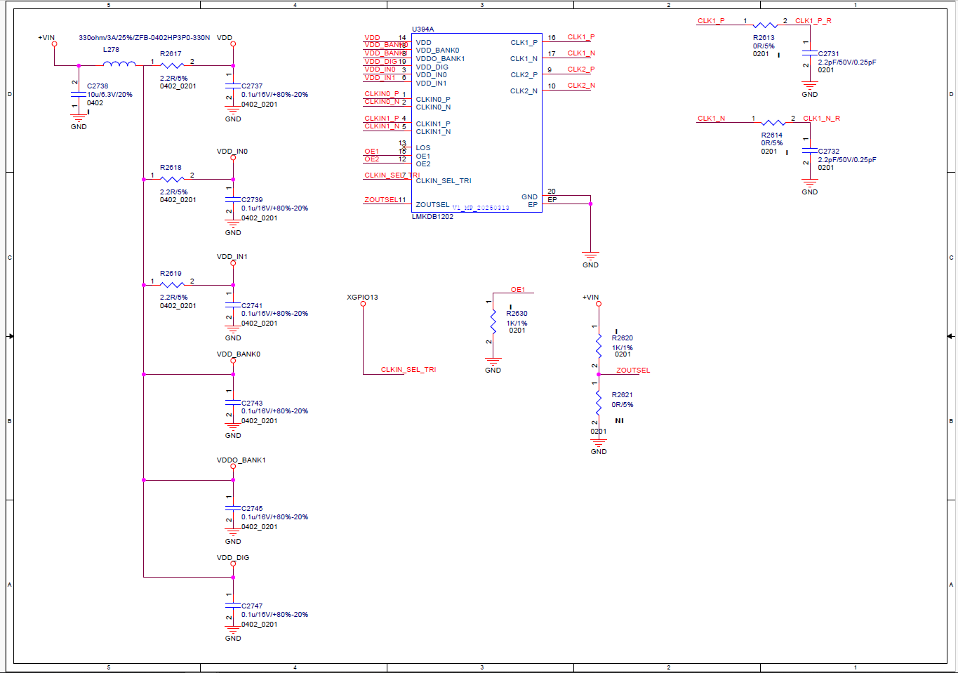
Since we are only using CLK 1 P/N, does that mean we don’t need to mount any components on it?
-> since our output only generates a single set of refclk, we only pull one OE
This is fine. You do not actually need to connect anything to the OE pins in order to enable the outputs, unless you want to do so dynamically, in which case you should follow the advice in the screenshot below (note that this only applies to OE1/Pin 15).
CLK_SEL will be determined as High (H) or Low (L) through our internal GPIO to allow CLKIN0/1 to output to the final output. (Please correct me if there are any errors.)
Just so you are aware, CLK_SEL is a 3-level select pin. Inputting a low voltage will drive CLKIN0 to all outputs, inputting a mid voltage will drive CLKIN0 to Bank 0 and CLKIN1 to Bank 1, and inputting a high voltage will drive CLKIN1 to all outputs.
For pin 15 OE's quesiton, I have confuse about the internal resistor, this pin is low-active, and datasheet mentioned there have internel pull-up. As I know if we need let this pin always low should be connect a pull-down resistor. But datasheet also mentioned can let this pin floating.
There is an internal pullup resistor. However, since you have connected OE1 to GND, it will be functional. You can leave this pin floating if you do not intend to use the CLK1 outputs. Otherwise, you should pull it down. Your schematic is correct and capable of having OE1 changed dynamically after startup - but if you do not plan on changing that state, then you are still fine.
Could you please tell me if the bead must be placed at 330 ohms, or can it be replaced with a 120 ohm/2A (0402)?
The bead must be selected such that its impedance at 100 MHz is 330 ohms. I would recommend using the ferrite bead instead of a resistor, as the ferrite bead is meant to reduce any transient coupling that could happen between supply rails.
The 2.2 pF load to GND mainly just reduces the output swing and provides high frequency transients a path to GND - you should be fine if you do not connect it.
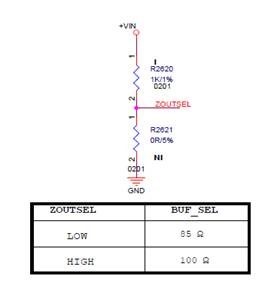
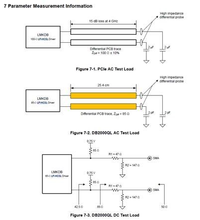
In the current application circuit, Pin 11 Zoutsel is set to H (100 Ω).
According to the measurement information in the datasheet, 100 Ω is paired with a 2µF capacitor, while 85 Ω is paired with a 2pF capacitor. Additionally, in the BOM list of the LMKDB1202 application circuit PDF, capacitors C21 to C24 are specified as 2pF on the EVB. On the EVB, it is also possible to select the Zoutsel pin as either H (100 Ω) or L (85 Ω).
However, only 2pF capacitors are used for C21 to C24 on the EVB. Given this, under what conditions is the 2µF capacitor mentioned in the datasheet applied?
The datasheet says that 2 uF loads are used in the 100 Ohms differential parameter measurement case, but this is a typo in our datasheet. The value in both cases is 2 pF.
2pF presents a lower load, and will result in a higher slew rate and drive strength than a 2 uF load. I would recommend using 2 pF capacitors to GND in the case of either output impedance.