This thread has been locked.

If you have a related question, please click the "Ask a related question" button in the top right corner. The newly created question will be automatically linked to this question.

LMK04828: LMK04828 - CLKino in SYSREF output

Part Number: LMK04828

Tool/software:

Dear Team,

In our schematic, we are using the LMK04828B, and our intention is to directly route CLKIN0 to the SYSREF path, and similarly, route CLKIN1 directly to the external VCXO path. That means input are expected to be directly connected to the clock distribution paths. Although we have attempted this configuration, we are not achieving the expected results. Could you please explain the correct steps to implement this setup?

  • Hello Sarathi, 
    Can you please share a block diagram or clock tree of what you're trying to implement? 

    For the most part using TICSpro helps with configuration. 
    You can also export your configuration as a .txt file for reference for your driver if you're using your own custom board and not the LMK04828EVM (eval board)
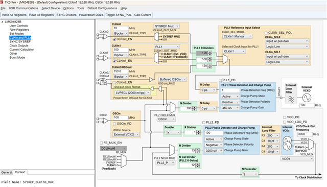
    Effectively your configuration what be following this topology. 

    Here CLKIN0 is routed to the SYSREF_MUX & CLKin1 is routed to PLL1 to drive an external VCXO. For this example I'll assume you want to drive a 100MHz VCXO. 
    You can also buffer the input to CLKin1 by setting CLKin1_OUT_MUX to 'Fin' which just bypasses PLL2 and has the device operate in buffer mode. At this point whatever signal you have at CLKin1 will be connected to the Clock distribution path. 

    For the SYNC/SYREF page your need SYSREF_CLKin0_MUX to be set to "From CLKin0' which sends your SYSREF signal at CLKin0 directly to the SYSREF Distribution path. 

    Best regards, 

    Vicente