This thread has been locked.

If you have a related question, please click the "Ask a related question" button in the top right corner. The newly created question will be automatically linked to this question.

LMK05318B-Q1: REFERENCE INPUT CHARACTERISTICS (PRIREF, SECREF) Input slew rate dV/dt value meaning

Part Number: LMK05318B-Q1

Tool/software:

Hi TI

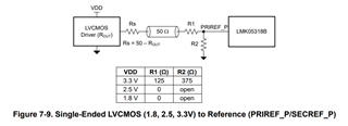
there is REFERENCE INPUT CHARACTERISTICS (PRIREF, SECREF) requirement in page 10 of datasheet, and the minimum recommended requirement of input slew rate  is 0.5V/ns described at note (14).

Q1: if now the input voltage level is 1.8V, does that mean the rise time of 1.8V voltage level is equal to 1.8V/0.5V/ns=3.6ns?

Q2: does that mean the minimum rise time requirement of 1.8V voltage level for the input PRIREF/SECREF is 3.6ns, correctly?

<

PARAMETER TEST CONDITIONS MIN TYP MAX UNIT
dV/dt              Input slew rate(14)                                                                          0.2    0.5 V/ns

(14) To meet the jitter performance listed in the subsequent sections of this data sheet, the minimum recommended slew rate for all
input clocks is 0.5V/ns. Phase noise performance begins to degrade as the clock input slew rate is reduced. However, the device
functions at slew rates down to the minimum listed. When compared to single-ended clocks, differential clocks (LVDS, LVPECL) are
less susceptible to degradation in phase noise performance at lower slew rates due to the common mode noise rejection. TI also
recommended to use the highest possible slew rate for differential clocks to achieve optimal phase noise performance at the device
outputs.

>

  • Hi TI

    add another question:

    Q3: Could please help to explain how to understand the PRIREF_CMOS_SLEW bit meaning at below table?

    Q4: What's the difference between Amplitude Detector Mode and CMOS Amplitude Detector Mode?

    1.33 R45 Register (Address = 0x2D) [Reset = 0x3]
    R45 is shown in Table 1-35.
    Return to the
    Summary Table.
    Table 1-35. R45 Register Field Descriptions

    Bit Field Type Reset Description
    7:5 RESERVED R 0x0 Reserved
    4 RESERVED R/W 0x0 Reserved
    3 SECREF_CMOS_SLEW R/W 0x0 SECREF input buffer slew rate
    0x0 = Select Amplitude Detector Mode
    0x1 = Select CMOS Amplitude Detector Mode
    2 PRIREF_CMOS_SLEW R/W 0x0 PRIREF input buffer slew rate
    0x0 = Select Amplitude Detector Mode
    0x1 = Select CMOS Amplitude Detector Mode
    1 SECREF_BUF_MODE R/W 0x1 SECREF buffer mode.
    0x0 = Set AC buffer hysteresis to 50 mV or enable DC buffer
    hysteresis
    0x1 = Set AC buffer hysteresis to 200 mV or disable DC buffer
    hysteresis
    0 PRIREF_BUF_MODE R/W 0x1 PRIREF buffer mode
    0x0 = Set AC buffer hysteresis to 50 mV or enable DC buffer
    hysteresis
    0x1 = Set AC buffer hysteresis to 200 mV or disable DC buffer
    hysteresis

  • Hi Wu,

    The recommended slew rate for input clock is 0.5 V/ns which means t_rise/fall is 3.6 ns. If you use faster slew rate (> 0.5 V/ns), the raise/fall time can be smaller than 3.6 ns. Since slew rate limits at 0.2 V/ns, the slowest rise/fall time is 1.8V/0.2V/ns = 9 ns max.

    There are two modes of xxxREF_CMOS_SLEW: amplitude detector mode and CMOS slew rate detector mode.

    In amplitude detector mode, the reference is considered valid if the signal swing is higher than the selected threshold.

    In CMOS slew rate detector mode, the detection method can be either slew rate detection or VIH / VIL detection.

    For slew rate detection, the input slew rate must be faster than 0.2 V/ns. For VIH / VIL detection, the input high level must be above 1.8 V and the low level must be below 0.6 V.

    The amplitude detection mode cannot be used for reference frequencies less than 5 MHz. If the reference frequency is above 5 MHz, then amplitude detection mode is recommended for differential input and the CMOS slew rate detection mode is recommended for single-ended input. If the input swing is too low (for example, the LVDS voltage swing is 400 mV, very marginal compared to the mininum threshold of amplitude detection mode), then amplitude detector can be disabled.

    -Riley

  • Hi Riley

    <For slew rate detection, the input slew rate must be faster than 0.2 V/ns. For VIH / VIL detection, the input high level must be above 1.8 V and the low level must be below 0.6 V.>

    Are there some margins for VIH voltage ,correctly? 

  • Hi Wu,

    It should not exceed 2.6V. If you're using 3.3V LVCMOS, you can add a voltage divider as shown here:

    -Riley