This thread has been locked.

If you have a related question, please click the "Ask a related question" button in the top right corner. The newly created question will be automatically linked to this question.

LMX2694EPEVM: Design method for LMX2694EPEVM

Part Number: LMX2694EPEVM
Other Parts Discussed in Thread: LMX2694-EP, LMX2582

Tool/software:

Hello, Dear TI Support Team

I have purchased the LMX2694-EP evaluation board and am evaluating it, but I have some questions, so I would like to post them here.

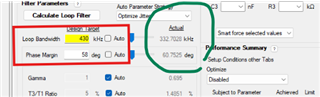
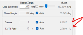
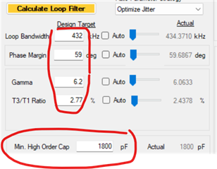
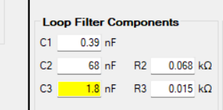
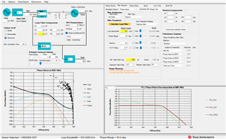
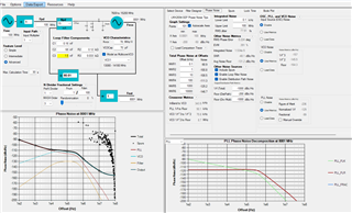
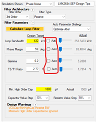
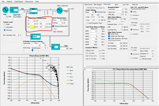
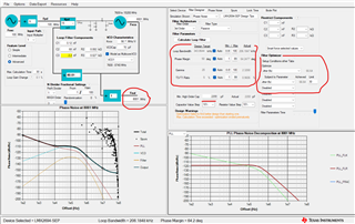
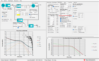
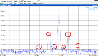
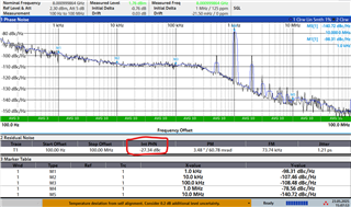
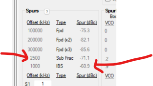
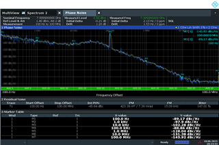
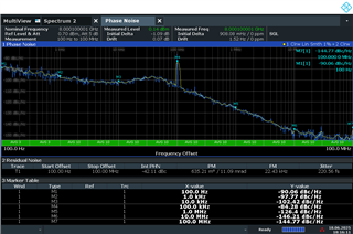
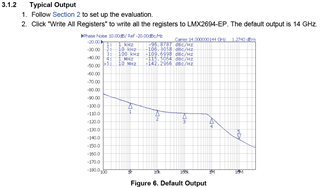
(1) Regarding the results listed in Figure 6 of the evaluation board PDF (snau245.pdf).
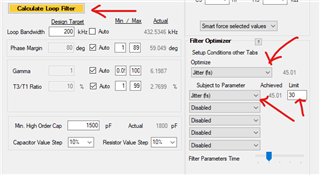
 I understand that the results in Figure 6 are obtained according to what is listed in Table 1. I also understand that the LoopFilter constants on the factory evaluation board are also the values listed in Table 1.

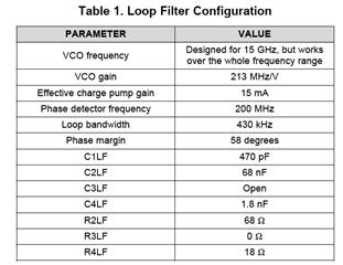
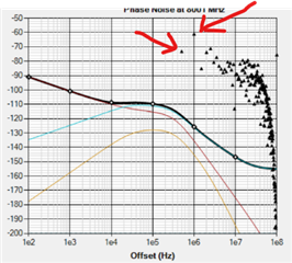
However, when I perform the design under the same conditions with your Sim software PLLatinum Sim, the LoopFilter constants show different values.

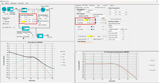
I would like to know the cause of this difference and the correct sim method (loop filter design method) to match the results of the evaluation board.

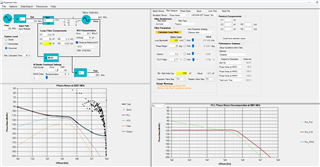
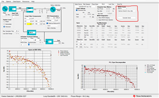
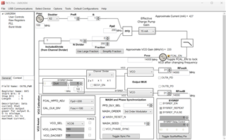
(2) In order to obtain the data described in Fig. 6, should I set up TICS Pro as shown in the following image?

R114	0x720000
R113	0x710000
R112	0x700000
R111	0x6F0000
R110	0x6E0000
R109	0x6D0000
R108	0x6C00F1
R107	0x6B0000
R106	0x6A0007
R105	0x694440
R104	0x680000
R103	0x670000
R102	0x660000
R101	0x650000
R100	0x640000
R99	0x630000
R98	0x620000
R97	0x610000
R96	0x600000
R95	0x5F0000
R94	0x5E0000
R93	0x5D0000
R92	0x5C0000
R91	0x5B0000
R90	0x5A0000
R89	0x590000
R88	0x580000
R87	0x570000
R86	0x560000
R85	0x550000
R84	0x540000
R83	0x530000
R82	0x520000
R81	0x510000
R80	0x500000
R79	0x4F0000
R78	0x4E0064
R77	0x4D0000
R76	0x4C000C
R75	0x4B0800
R74	0x4A0000
R73	0x49003F
R72	0x480001
R71	0x470080
R70	0x46C350
R69	0x450000
R68	0x4403E8
R67	0x430000
R66	0x4201F4
R65	0x410000
R64	0x401388
R63	0x3F0000
R62	0x3E0322
R61	0x3D00A8
R60	0x3C09C4
R59	0x3B0001
R58	0x3A8001
R57	0x390020
R56	0x380000
R55	0x370000
R54	0x360000
R53	0x350000
R52	0x340420
R51	0x330080
R50	0x320000
R49	0x314180
R48	0x300300
R47	0x2F0300
R46	0x2E07FD
R45	0x2DC8DF
R44	0x2C1F23
R43	0x2B0000
R42	0x2A0000
R41	0x290000
R40	0x280000
R39	0x2700C8
R38	0x260000
R37	0x258404
R36	0x240046
R35	0x230004
R34	0x220000
R33	0x211E21
R32	0x200393
R31	0x1F03EC
R30	0x1E318C
R29	0x1D318C
R28	0x1C0488
R27	0x1B0002
R26	0x1A0DB0
R25	0x190624
R24	0x18071A
R23	0x17007C
R22	0x160001
R21	0x150401
R20	0x14F048
R19	0x1327B7
R18	0x120064
R17	0x11012C
R16	0x100080
R15	0x0F064F
R14	0x0E1E70
R13	0x0D4000
R12	0x0C5001
R11	0x0B0018
R10	0x0A10D8
R9	0x091604
R8	0x082000
R7	0x0700B2
R6	0x067802
R5	0x0503E8
R4	0x040E43
R3	0x030642
R2	0x020500
R1	0x010809
R0	0x00211C

Please answer the above two questions.

  • Hi Naohiro-san,

    Your design target is 430kHz but the actual is 332.7kHz, so the loop filter is different from EVM default.

    This is because you haven't set the target for Gamma and T3/T1 ratio.

    EVM default:

    Set the same value as your target:

    Then you will get the loop filter very similar to EVM.

  • Dear Noel Fung,
    Thank you for your response.
    I understand that the issue was due to not setting the Gamma and T3/T1 parameters.
    I would appreciate it if you could answer the following questions, as well as respond to question (2) from my initial post.
    (1) I apologize for my lack of understanding, but could you please explain what the Gamma parameter and the T3/T1 parameter represent?
    (2) When I set the parameters as you suggested, the simulation shows C1 as 0.39pF, but the datasheet lists C1LF as 0.47nF (470pF). Additionally, R3 in the
    simulation is 15Ω, while the datasheet shows R4LF as 18Ω. Could you please explain the reason for these discrepancies?
    Thank you for your assistance.
    Best regards.
  • Hi Naohiro-san,

    This is a 3rd order loop filter, so there are three poles, T1, T2 and T3. 

    T3/T1 is the ratio of the pole T3 to the pole T1. Higher percentage means higher attenuation. As a result, higher loop bandwidth is not possible. 

    Gamma = 1 yields max. phase margin at the loop bandwidth. If you want fast lock time, make this close to 1. Higher Gamma may produce a flatter inband respond but increase lock time.

    390pF vs 470pF and 15Ω vs 18Ω literally has no obvious effect on the loop characteristic. Simulation provides suggested values, actual implementation picks the closest market available values. 

    You will get Figure 6 result if you use the "Default Configuration" from TICS Pro.

    Your configuration modified some configurations but it is fine, you should get the same result as Figure 6.

    Please note, Figure 6 was taken with a very low noise reference clock. Suggested clock source are Wenzel OCXO or SMA100B.

  • Thanks for the reply Noel Fung

    Thanks for the explanation about T3/T1 and Gamma parameters.

    By actually swinging the parameters and verifying the sim results, I now understand the nuances of what you are saying.

    I also now understand the difference between the constants. So it was a matter of market availability.

    I now understand that with a similar setup, I can get the same results as in Figure 6.

    Let me ask a follow-up question.

    I am currently looking to run this evaluation board at 8 GHz and 8.001 GHz.
    (I would like to run this PLL in Fractional mode.)
    The parameter that I want to optimize with the highest priority is SNR. Can I find the optimal C/N by using the following Sim settings? I would appreciate any suggestions for improvement.
    I would like to determine the constants of the Loop Filter based on the results obtained from this sim.

    Also, when performing optimization here, could you please tell me whether it is better to uncheck the Auto checkbox in the red box below or to check the Auto checkbox?

    Please answer the above questions.

    Thank you for your assistance.
    Best regards.
  • Hi Noel Fung.

    I have an additional question, which I would like to ask you to answer together with the above question.

    I have found the Loop Filter at 8001GHz using PLLatinum.
    The constants are shown in the image below.

    When I changed the constants on the evaluation board to be the same as the sim result based on this result, the phase noise was different from the sim result as shown in the image below.


    I would like to know the cause of this difference.

  • Hi Naohiro-san,

    We have a PLL Sim training video in below link.

    https://www.ti.com/video/6330930382112?keyMatch=pllatinum%20sim&tisearch=universal_search

    Better SNR means lower phase noise or jitter. Usually a wider loop bandwidth + higher phase margin can return lower jitter. 

    We can manually type the four target parameters and click the Calculate Loop Filter button to get the suggested values and actual loop performance.

    We can uncheck the boxes and move the slide bar to quickly see the effect.

    We can also provide a target jitter to the tool, it will come up with the best possible configuration for us.

    The video has the details.

    Your plot shown the loop bandwidth is just 50kHz with a small phase margin. Likely this is due to wrong component values are populated.

  • Hi Noel Fung.

    Thank you for your reply.

    I understood that the jitter parameter is the most effective for SNR.

    Based on the results of the training video, I further increased the phase margin and loop bandwidth from 50kHz to 206kHz.
    In order to achieve good SNR, we designed the system as shown in the following image.
    The jitter parameter of Filter Otimizer is set to 30.
    Loop Bandwidth, Phase Margin, Gamma, and T3/T1 Ratio were set to Auto
    - MASH Seeds was set to Optimize Seeds for Spur Jitter and the calculation was performed
    As a result, SNR of -49.5 dBc/Hz was obtained.

    The simulation results did not show any spurious signal, but the actual measurement results showed a 1 MHz spurious signal.

    (1)Please tell me the cause of this 1MHz spurious.

    In addition, I obtained a result of -49.5dBc/Hz for SNR with Sim, but it was -27.34dBc/Hz in the actual measurement.

    (2)Please tell me the cause of the difference between the Sim and measured results.

    Based on the Sim results, we changed the parameters of the evaluation board as follows.
    The following are the part names of the evaluation board and the changed parameters.
    C1LF: 0.47nF -> 0.12nF
    C2LF: 68nF -> No change
    C3LF: 1.8nF -> 2.2nF
    R2LF: 0.068kΩ -> 0.082kΩ
    R4LF: 0.018kΩ -> 0.027kΩ

    Please reply to questions (1) and (2).
    Also,Please answer the above questions.

  • Hi Naohiro,

    The sim already told you there are spurs:

    With 100MHz input and 8001MHz output, for sure there will be Integer Boundary Spurs (IBS) at 1MHz. Fractional spurs is also 1MHz. Sub-fractional spurs appear at 1/2, 3/2 of fractional spurs frequency. 

    The sim can predict the spurs frequency but not able to accurately predict the spurs level as this is very much depends on the chip layout. The spurs level also depends on the input clock format and level. 

    You may read LMX2582 datasheet, section 8.1, for details of spurs.

    Your measurement integrated all the noise between 100Hz and 100MHz, including the spurs, so the jitter and SNR is bad. If you omit spurs in your measurement, you should get SNR close to simulation. 

    To reduce this spurs, use smaller charge pump current, use square wave input clock, use a weird PLL NUM such as 10000001.

  • Hi Noel Fung.

    Thanks for the reference on the factors of spurious components.

    To reduce this spurious component, I am currently thinking of using a clock buffer to input differential input signals.

    (1) Is it possible to input LVPECL signal format?
    Is it possible to input LVPECL signals or only LVDS?

    (2) Is it possible to input differential signals directly to the factory evaluation board? Is there anything we need to change on our end?

    Please answer the above two questions.

  • Hi Naohiro-san,

    Both LVDS and LVPECL are acceptable.

    The eval board is default to single-ended input, you need to modify it for differential input. See EVM user's guide for details.

    If the input is LVPECL, the modification is same as above diagram except that R31 and R32 should be 0.1µF capacitor.

  • Hi Noel Fung.

    By using LVPECL as input, the integrated C/N value has improved.

    Thank you very much.

    Question 1) Please tell me why spurious improves with differential signal input.

    Question 2) In TI PLLatinum, when I try to analyze up to kHzOrder like 7689.33MHz, my PC gets stuck. Please tell me a simple method to derive an approximate value.

    Please answer the above two questions.

  • Hi Naohiro-san,

    1. Spurs are due to modulation to the VCO, the modulation signals come from different paths. The mechanism of modulation signal generation is complex and tricky. I believe any non-linearity, mismatch or offset create the modulation signals. Our observation is that a differential square wave reference clock tends to return less spurs.

    2. this happen very often if we enable spurs in PLL Sim. this is due to extensive calculation for spurs in the background. It will show "not responding" but in fact it is still running. If you can wait for some time, it will resume to normal after all calibrations are done.

  • Hi Noel Fung.

    I understood that differential signals tend to be better for spurious, and that the clear mechanism is complex and not obvious.

    I have a question about Sim and actual measurement in 0.1 MHz increments.

    Sim and actual measurements were made at 7999.9MHz~8001.1MHz. The measurement results are as follows.

    The signal used for the measurement was the LVPECL signal.

    The following are the measurement results at CP15mA.

    The following are the measurement results at CP3mA.

    Ideally, we would like to achieve -46dBc/Hz or less.

    Can this result be any better?

  • Hi Naohiro-san,

    With 100kHz step, for sure there will be spurs at multiples of 100kHz offset.

    Reducing charge pump current can reduce the spurs level. However, the loop bandwidth will also be reduced. As a result, inband noise will be higher. 

    We could also try using different order MASH. Third or forth order MASH, in general, can randomize spurs better but also increase phase noise. 

    We may try 4th order loop filter, hopefully can provide some degree of spurs reduction.

    We may also play around the PFD_DLY_SEL register to optimize phase noise.

    We can also try using a bigger PLL_DEN such as 10000001. 

    In short, it is more or less a trial and error fashion to optimize overall phase noise or SNR.