This thread has been locked.

If you have a related question, please click the "Ask a related question" button in the top right corner. The newly created question will be automatically linked to this question.

LMK00304: 1:4 LVDS fan-out configuration — 100 MHz LVDS input, LVDS outputs

Part Number: LMK00304

Tool/software:

Hello Team,

I’d like to double-check my clock-distribution setup.

I have a single 100 MHz LVDS clock that I need to fan out to several PCIe devices (SSDs, controller, etc.).

  • Reference input: CLKin0, fed with the 100 MHz LVDS signal

  • Outputs: Four channels, each configured for LVDS

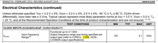
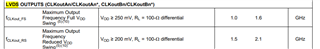
The datasheet lists a minimum LVDS frequency of 1 GHz—can you confirm whether that applies to this use case? Also, can you confirm that the device will simply pass the input frequency through, giving four 100 MHz outputs from the 100 MHz input?

Thank you!

  • Hello Erdem, 
    This device works form DC up to 3.1GHz. 

    The spec you're probably confusing this with is the following: 

    This spec is guaranteeing full VOD swing from 1GHz to 1.6GHz

    This is not the minimum input frequency. 

    This device will work if you feed it a 100MHZ LVDS signal with the correct termination. 

    Best regards, 

    Vicente 

  • Hi Vincente,

    Thank you for your reply.

    Could you help me review the schematic and the LVDS termination? The 100 MHz LVDS reference clock (REF0) originates from U1900 and is routed to the PCIe devices as LVDS. Please let me know if the termination looks correct.

    Best regards,

  • Hi Erdem,

    I took a look over your schematic and you have configured the device appropriately for inputting an LVDS signal to CLKin0 and outputting an LVDS signal. 

    However, you do not need differential terminations on both the receiver and transmitter side - the recommendation is only to differentially terminate with 100 ohms on the input. 

    Furthermore, I am a bit confused by the pullups and pulldowns you have (R1925-1926, R1931-1932, R1927-1930, and R1937-R1940). Can you clarify why those are there? I believe they may result in improper and unexpected functionality.

    Thanks,

    Michael

  • Thank you very much for your response.

    First, let me explain the purpose of these resistors:

    R1925–R1926 and R1931–R1932 :
    These resistors help bring the DC offset of the differential pairs closer together. This alignment reduces the hysteresis and ensures proper operation. Please refer to the attached image—this is based on a comment found in the same forum under the LMK00304 topic: Input LVDS AC Coupling.

    R1927–R1930 and R1937–R1940:
    These resistors provide the necessary bias voltage to the receivers. Since the signals are AC-coupled, the DC component is blocked, and these resistors are essential to establish a proper common-mode voltage at the receiver side.

  • Hi Erdem,

    I understand that you are planning on AC coupling all of your LVDS signals, but that is not the way I would provide a bias voltage. The appropriate thing to do would be to make sure that, after AC coupling, all of the signals are brought to the common mode voltage (typically, VDD/2). You can do this by putting both pull up and pull down resistors (of equal value) on each line. It is not appropriate to pull the positive end up to VDD and the negative end to GND - this will result in the receiver only seeing a high signal, and railing out.

    Thanks,

    Michael

  • I took it from How to Terminate LVDS Connections with DC and AC Coupling but of course happy apply your recommendation

  • Hi Erdem,

    Thank you for bringing that to my attention! I was neglecting the impacts of that 100 Ohm differential termination (like I said earlier, the best practice is typically to only place this termination on the receiver side, and if that were to be the case then my recommendation would be the appropriate way to bias it). 

    If you plan to leave the 100 Ohm termination on the transmitter side, then the biasing configurations for R1927–R1930 and R1937–R1940 will be fine - but we recommend only terminating on the receiver side in order to reduce reflections.

    Thanks,

    Michael