This thread has been locked.

If you have a related question, please click the "Ask a related question" button in the top right corner. The newly created question will be automatically linked to this question.

LMX2594: lmx2594 frequency unstable,drift

Part Number: LMX2594

Tool/software:

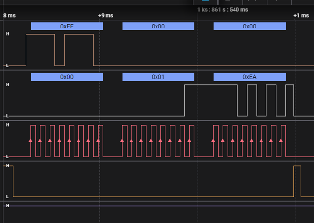
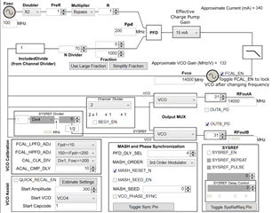
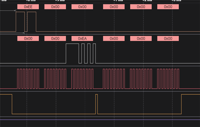
I read R110 to determine lock status.  The readback value is 0x01EA.

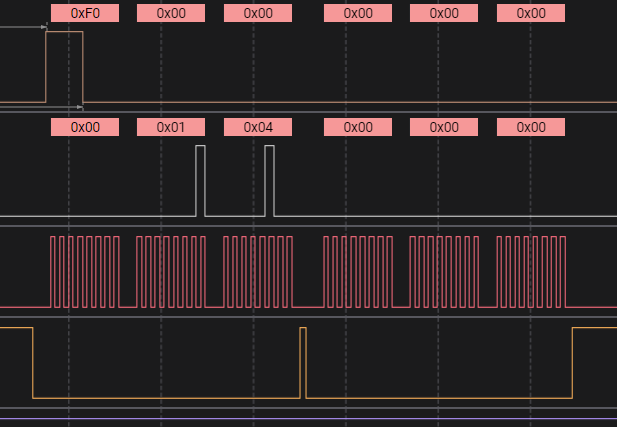
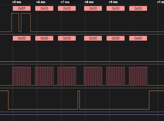
I am not sure where wrong,but I have this file1121.test.tcs

this is my teamMate setting , but it seem some mistake,and i am not RF expert.

i only can check the value of R110 register.

please help me find the bug ,thx

  • Hi Yan Ting,

    Your configuration is fine. 

    First of all, make sure you can program the device. To verify this, after Vcc power up the device, program POWERDOWN=1, if there is significant current change, that mean programming is fine.

    Then follow below procedure to program the device.

    1. Make sure you have a valid input clock

    2. Program RESET = 1

    3. Program all registers in descending order. That is, from the highest address to the lowest address, the last register to program is R0.

    4. This step is optional. Program R0 one more time.

  • hello ,Noel Fung.

    But the register R110 value is 1EA that mean D10,D9=0 , it mean unlock.

    my command with spi is 

    void initial()
    {
    sendSPI(0x62, 0x02, 0x00);
    sendSPI(0x63, 0x00, 0x00);
    sendSPI(0x66, 0x3F, 0x80);
    sendSPI(0x67, 0x00, 0x00);
    sendSPI(0x51, 0x00, 0x00);
    sendSPI(0x52, 0x1E, 0x00);
    sendSPI(0x53, 0x00, 0x00);
    sendSPI(0x54, 0x00, 0x01);
    sendSPI(0x55, 0xD3, 0x00);
    sendSPI(0x56, 0x00, 0x00);
    sendSPI(0x4E, 0x00, 0x03);
    sendSPI(0x4F, 0x00, 0x26);
    sendSPI(0x50, 0x66, 0x66);
    }
    void Set_LO()
    {
    sendSPI(0x4B, 0x09, 0x00);
    sendSPI(0x22, 0x00, 0x00);
    sendSPI(0x24, 0x00, 0x2A);
    sendSPI(0x2D, 0xC8, 0xDF);
    sendSPI(0x22, 0x00, 0x00);
    sendSPI(0x24, 0x00, 0x32);
    }
    void Reset()
    {
    // block 1
    sendSPI(0x70, 0x00, 0x00);
    sendSPI(0x6F, 0x00, 0x00);
    sendSPI(0x6E, 0x00, 0x00);
    sendSPI(0x6D, 0x00, 0x00);
    sendSPI(0x6C, 0x00, 0x00);
    sendSPI(0x6B, 0x00, 0x00);
    sendSPI(0x6A, 0x00, 0x00);
    sendSPI(0x69, 0x00, 0x21);
    sendSPI(0x68, 0x00, 0x00);
    sendSPI(0x67, 0x00, 0x00);
    sendSPI(0x66, 0x00, 0x00);
    sendSPI(0x65, 0x00, 0x11);
    // block 2
    sendSPI(0x64, 0x00, 0x00);
    sendSPI(0x63, 0x00, 0x00);
    sendSPI(0x62, 0x00, 0x00);
    sendSPI(0x61, 0x08, 0x88);
    sendSPI(0x60, 0x00, 0x00);
    sendSPI(0x5F, 0x00, 0x00);
    sendSPI(0x5E, 0x00, 0x00);
    sendSPI(0x5D, 0x00, 0x00);
    sendSPI(0x5C, 0x00, 0x00);
    sendSPI(0x5B, 0x00, 0x00);
    sendSPI(0x5A, 0x00, 0x00);
    sendSPI(0x59, 0x00, 0x00);
    // block 3
    sendSPI(0x58, 0x00, 0x00);
    sendSPI(0x57, 0x00, 0x00);
    sendSPI(0x56, 0x00, 0x00);
    sendSPI(0x55, 0x00, 0x00);
    sendSPI(0x54, 0x00, 0x00);
    sendSPI(0x53, 0x00, 0x00);
    sendSPI(0x52, 0x00, 0x00);
    sendSPI(0x51, 0x00, 0x00);
    sendSPI(0x50, 0x00, 0x00);
    sendSPI(0x4F, 0x00, 0x00);
    sendSPI(0x4E, 0x00, 0x03);
    sendSPI(0x4D, 0x00, 0x00);
    // block 4
    sendSPI(0x4C, 0x00, 0x0C);
    sendSPI(0x4B, 0x08, 0x00);
    sendSPI(0x4A, 0x00, 0x00);
    sendSPI(0x49, 0x00, 0x3F);
    sendSPI(0x48, 0x00, 0x01);
    sendSPI(0x47, 0x00, 0x81);
    sendSPI(0x46, 0xC3, 0x50);
    sendSPI(0x45, 0x00, 0x00);
    sendSPI(0x44, 0x03, 0xE8);
    sendSPI(0x43, 0x00, 0x00);
    sendSPI(0x42, 0x01, 0xF4);
    sendSPI(0x41, 0x00, 0x00);
    // block 5
    sendSPI(0x40, 0x13, 0x88);
    sendSPI(0x3F, 0x00, 0x00);
    sendSPI(0x3E, 0x03, 0x22);
    sendSPI(0x3D, 0x00, 0xA8);
    sendSPI(0x3C, 0x00, 0x00);
    sendSPI(0x3B, 0x00, 0x01);
    sendSPI(0x3A, 0x90, 0x01);
    sendSPI(0x39, 0x00, 0x20);
    sendSPI(0x38, 0x00, 0x00);
    sendSPI(0x37, 0x00, 0x00);
    sendSPI(0x36, 0x00, 0x00);
    sendSPI(0x35, 0x00, 0x00);
    // block 6
    sendSPI(0x34, 0x08, 0x20);
    sendSPI(0x33, 0x00, 0x80);
    sendSPI(0x32, 0x00, 0x00);
    sendSPI(0x31, 0x41, 0x80);
    sendSPI(0x30, 0x03, 0x00);
    sendSPI(0x2F, 0x03, 0x00);
    sendSPI(0x2E, 0x07, 0xFC);
    sendSPI(0x2D, 0xC0, 0xDF);
    sendSPI(0x2C, 0x1F, 0xA3);
    sendSPI(0x2B, 0x00, 0x00);
    sendSPI(0x2A, 0x00, 0x00);
    sendSPI(0x29, 0x00, 0x00);
    // block 7
    sendSPI(0x28, 0x00, 0x00);
    sendSPI(0x27, 0x03, 0xE8);
    sendSPI(0x26, 0x00, 0x00);
    sendSPI(0x25, 0x04, 0x04);
    sendSPI(0x24, 0x00, 0x46);
    sendSPI(0x23, 0x00, 0x04);
    sendSPI(0x22, 0x00, 0x00);
    sendSPI(0x21, 0x1E, 0x21);
    sendSPI(0x20, 0x03, 0x93);
    sendSPI(0x1F, 0x43, 0xEC);
    sendSPI(0x1E, 0x31, 0x8C);
    sendSPI(0x1D, 0x31, 0x8C);
    // block 8
    sendSPI(0x1C, 0x04, 0x88);
    sendSPI(0x1B, 0x00, 0x02);
    sendSPI(0x1A, 0x0D, 0xB0);
    sendSPI(0x19, 0x0C, 0x2B);
    sendSPI(0x18, 0x07, 0x1A);
    sendSPI(0x17, 0x00, 0x7C);
    sendSPI(0x16, 0x00, 0x01);
    sendSPI(0x15, 0x04, 0x01);
    sendSPI(0x14, 0xE0, 0x48);
    sendSPI(0x13, 0x27, 0xB7);
    sendSPI(0x12, 0x00, 0x64);
    sendSPI(0x11, 0x01, 0x2C);
    // block 9
    sendSPI(0x10, 0x00, 0x80);
    sendSPI(0x0F, 0x06, 0x4F);
    sendSPI(0x0E, 0x1E, 0x70);
    sendSPI(0x0D, 0x40, 0x00);
    sendSPI(0x0C, 0xC5, 0x01);
    sendSPI(0x0B, 0x00, 0x18);
    sendSPI(0x0A, 0x10, 0xD8);
    sendSPI(0x09, 0x16, 0x04);
    sendSPI(0x08, 0x20, 0x00);
    sendSPI(0x07, 0x40, 0xB2);
    sendSPI(0x06, 0xC8, 0x02);
    sendSPI(0x05, 0x50, 0xC8);
    // block 10
    sendSPI(0x04, 0x0A, 0x43);
    sendSPI(0x03, 0x06, 0x42);
    sendSPI(0x02, 0x05, 0x00);
    sendSPI(0x01, 0x08, 0x08);
    sendSPI(0x00, 0x25, 0x1C);
    }
    code is

      initial();
      delay(10);
      Reset();
      delay(10);
      Set_LO();
      delay(10);

    or maybe command is wrong?
  • comment:

    my ref clock is use 100Mhz and ppm is 25-50 ppm ,is it cause unstable or unlock?

  • This is my R110 register response

  • I am sure I can see the RF signal ,IF signal is 1.8Ghz and I can see the 13.3GHZ RF signal on Spectrum analysis.

    and current about 400mA, but the frequency like register data 0x1EA ,look like unstable. and drift....

  • Hi Yan Ting,

    Based on your code, your configuration has output B powerdown and 7GHz at output A. 

    MUXOUT_LD_SEL is set to lock detect output, did you measure logic HIGH at MUXout pin?

    What is the Vtune voltage? If it is locked, it should be around 1.3V. 

    Can you share your schematic?

  • No, although I select MUXout of LD_SE pin, I can still get Readback signal when I give command, and its value is 0x1EA. I didn't measure Vtune voltage, but I saw it is always low in logic analysis, so I think it is just close to 0V.

  • I didn't have schematic, because this is someone design for me , I only can use software modify and test, to try function test... but when I try I found it is unstable and drift...

  • Singal like this look like unstable  and unlocked

  • Th is I read R111,R112 register Value. I am sure that Vtune voltage is near 9mv and Vcal freq look like zero...

    All the data information is proove that function look like failure only  converter a high freq ....

    So I think someone give me a code only can see a high frequency converter but it drift too much,

    I can't use this to send wirelses singal ...such qpsk or each other format of wireless singal...

    I have idea that could u supply a one or more demo code of register that Can Build 14GHz frequency and could lock frequency to me?

    Because I only need IF singal ia almost 1.8G~3Ghz ,and I neet to up_converter to 14GHz , only need this function.

    Because I search this 14Ghz demo code , Information is too less... I only need a correct demo and register table.

    I only modify the register and try I can know the function is correctly immediately.... please help .

    I only remain about 12 hours to finish this project ,so I need quickly....

  • Hi Yan Ting,

    Here is the code.

    R112	0x700000
    R111	0x6F0000
    R110	0x6E0000
    R109	0x6D0000
    R108	0x6C0000
    R107	0x6B0000
    R106	0x6A0000
    R105	0x690021
    R104	0x680000
    R103	0x670000
    R102	0x660000
    R101	0x650011
    R100	0x640000
    R99	0x630000
    R98	0x620000
    R97	0x610888
    R96	0x600000
    R95	0x5F0000
    R94	0x5E0000
    R93	0x5D0000
    R92	0x5C0000
    R91	0x5B0000
    R90	0x5A0000
    R89	0x590000
    R88	0x580000
    R87	0x570000
    R86	0x560000
    R85	0x550000
    R84	0x540000
    R83	0x530000
    R82	0x520000
    R81	0x510000
    R80	0x500000
    R79	0x4F0000
    R78	0x4E0003
    R77	0x4D0000
    R76	0x4C000C
    R75	0x4B0800
    R74	0x4A0000
    R73	0x49003F
    R72	0x480001
    R71	0x470081
    R70	0x46C350
    R69	0x450000
    R68	0x4403E8
    R67	0x430000
    R66	0x4201F4
    R65	0x410000
    R64	0x401388
    R63	0x3F0000
    R62	0x3E0322
    R61	0x3D00A8
    R60	0x3C0000
    R59	0x3B0001
    R58	0x3A9001
    R57	0x390020
    R56	0x380000
    R55	0x370000
    R54	0x360000
    R53	0x350000
    R52	0x340820
    R51	0x330080
    R50	0x320000
    R49	0x314180
    R48	0x300300
    R47	0x2F0300
    R46	0x2E07FD
    R45	0x2DC8DF
    R44	0x2C1FA3
    R43	0x2B0000
    R42	0x2A0000
    R41	0x290000
    R40	0x280000
    R39	0x2703E8
    R38	0x260000
    R37	0x250404
    R36	0x240046
    R35	0x230004
    R34	0x220000
    R33	0x211E21
    R32	0x200393
    R31	0x1F03EC
    R30	0x1E318C
    R29	0x1D318C
    R28	0x1C0488
    R27	0x1B0002
    R26	0x1A0DB0
    R25	0x190C2B
    R24	0x18071A
    R23	0x17007C
    R22	0x160001
    R21	0x150401
    R20	0x14E048
    R19	0x1327B7
    R18	0x120064
    R17	0x11012C
    R16	0x100080
    R15	0x0F064F
    R14	0x0E1E70
    R13	0x0D4000
    R12	0x0C5001
    R11	0x0B0018
    R10	0x0A10D8
    R9	0x091604
    R8	0x082000
    R7	0x0740B2
    R6	0x06C802
    R5	0x0500C8
    R4	0x040A43
    R3	0x030642
    R2	0x020500
    R1	0x010808
    R0	0x00251C
    

    This is configuration.

    Did you verify the 100MHz input clock? Does it look good?

  • no....seems hardware is wrong , I try you give me the code.

    and register is change 0EA from 1EA....

    I don't have any idea and clock we use this.... 100Mhz ak5 

  • ask a question, if my ref clcok is not exist, do i see the IF singal up-converter to 13.3 RF singal is it possible?

  • Hi Yan Ting,

    AK5 is the reference clock, LVDS output, the connection is correct but the layout is very bad. 

    If you have a differential probe, probe across resistor R8, you should get 100MHz clock with 700mVpp to 800mVpp square wave signal. 

    We can program the device without a reference clock. To lock the PLL/VCO needs a valid reference clock, otherwise there will be output but the frequency is not correct.

  • I try to measure use osc with r8 , but I seem only see 1.2 voltage and not like square wave , maybe clock is didn't work... so I think that pll no locked maybe is no ref clock. But it still up converter...