LMK04828: LMK04828 Oscillator Circuit Design

Part Number: LMK04828
Other Parts Discussed in Thread: , AFE7900EVM

Tool/software:

Hello TI Team, 

We are using LMK04828 in one of our design, we need to know the two things about oscillator input pins. 

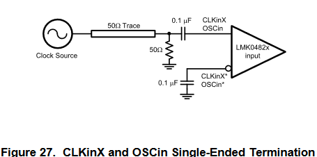
1. What is the maximum allowable input current on OSCINp and OSCINn pins for the single single ended clock input LVCMOS? For differential mode it is +/-5mA as per datasheet, for LVCMOS, how much it would be?

2. What is the input impedance on OSCINp and OSCINn? 

we are using the SiTime Oscillator, which is default operating at 3V3 supply with the passive circuit design we shall be making input clock logic level within acceptable limit of LMK i.e 0.2 ~ 2.4V as per datasheet. 

For precise components selection we wish to know the above two points. 

  • The differential input current rating refers to the current across the antiparallel diode stack between P and N pins; hence the VID limit of about three diode forward voltages. The 2.4Vpp single-ended AC-coupled limit is to ensure that, regardless of PVT spread for the self-biasing of the input stage, the signal swing does not saturate the amplifier (which could degrade slew rate and phase noise performance).

    For single-ended LVCMOS, as long as the other end is capacitively coupled to GND and the CMOS signal respects the absolute minimum/maximum input voltage for the device, there shouldn't be a case where the antiparallel diodes are ever continuously active at currents exceeding the rated current, so the ±5mA constraint will be satisfied (treat this as ±5mARMS). That just leaves the 2.4Vpp single-ended constraint, which as far as I can tell is satisfied by the schematic snippet (I don't see it on the web any more, but have an extremely low-resolution copy in my inbox - it may have been removed?) - though I think the amplitude of your 3.3V signal is attenuated much more than needed (down to about 0.9Vpp), and you could probably afford to increase the impedance of the 130/50 biasing. You could approximately match the expected 50Ω impedance with a 100Ω/100Ω biasing circuit, and maybe 25Ω in series with the driver (as suggested in the SiT5347 datasheet, presumably to accommodate the output impedance of the driver) - this would be about 1.65Vpp input signal, which is well within the rated range for single-ended AC-coupled drive. You should probably check with SiTime for the minimum rated AC-coupled load impedance before settling on a final value, but my point is, you have a lot of room for a larger signal to the LMK04828 if you'd like to use it.

    edit to add: OSCINp and OSCINm are high-impedance at DC. At around 100MHz, they appear to be quite close to 50Ω real, somewhere between 1.3pF and 1.8pF imaginary.

  • Hi Derek, 

    Thanks for the clarity. 

    Also, a quick check on TI clock buffer ICs solutions that can be used to cater clock interface requirements from external source with minimum design components. 

    Please consider single ended AC coupled LVCMOS logic for LMK. 

    Regards, 

    Garima R. 

  • Hello Derek, 

    As per reply on 27th June, If the input impedance for the OSCIN pins is 50E, then as per electrical rules maximum current will exceed 5mA on these pins which is mentioned in the datasheet absolute maximum table. 

    Vmax = 2.4V R = 50E and I = 48mA (max) 

    Could you provide clarification on this if we are missing out something. 

    Regards, 

    Garima R. 

  • The current would be going into a discrete 50Ω resistor, rather than into the device pins, because OSCin should be AC-coupled. I'm suggesting a scheme similar to Figure 27 in the datasheet, only with a 25Ω series resistor between the clock source and the 50Ω trace to help match the source impedance from the driver.

    Apologies for missing the buffer check question earlier. I don't think an additional clock buffer device for interfacing would be necessary, given that the suggested termination with the series source resistor could be applied as-is with an LVCMOS source.

  • Hello Derek, 

    Sorry for late response. 

    Understood the pointy here, thanks. 

    I am curious that why we have used the highlighted circuit in the design?

    First, The Y2 is 3.3V logic and optional DC offset circuit is there (R314). Is this offset needed purposely for any future application? Also do we need to add it in design? 

    Second, The purpose of R308? 

    Regards, 

    Garima R. 

  • I actually don't recognize this schematic - is it a reference design?

    130Ω and 82Ω sound like values that form an LVPECL termination (3.3V * 82/(130+82) = about VCC - 2V; 130 || 82 = about 50Ω). I wonder if the intention was to replace R309 and C239 with 0Ω, and DNP R316, to provide LVPECL DC-termination - I know on the LMK04828BEVM we allow a 4-pin and a 6-pin variant of the VCXO, which can be populated for either LVPECL or LVCMOS styles, so maybe something similar was done on this board. Or maybe OSCN net connects elsewhere (such as an off-board connector) and R308 value should be used to populate R316, with C239 and backward DNP.

    In any case, for single-ended LVCMOS coupling, I think both R314 and R308 may be safely omitted from the final design.

  • Hello Derek, 

    Thanks for the detailed response. 

    The above snap is from the AFE7950EVK design. 

    As you said it seems LVPECL termination option as the nets are not going to any off board connector. 

    Regards, 

    Garima R. 

  • Request you to refer the circuit in DC135A_AFE7900EVM

    One last doubt on the above circuit, for AC coupling we believe a single 0.1uF would be sufficient as datasheet suggests but in EVM there are two being used C239 and C245. Additionally in the EVM clock is sourced on negative pin with C250 =12pF in parallel. 

    Regards, 

    Garima R. 

  • It depends on the DC output current tolerance of the source oscillator, as I mentioned before. If SiTime says their oscillator can handle the DC current from the resistors used, I think C239 could be replaced with a wire without any problems. On the other hand, if SiTime says the DC current is too much for their oscillator, C239 creates the appropriate voltage division without a DC load on the oscillator.

    C250 I'm not sure about. I think it was intended for rolling off some of the high frequency CMOS content, as it was injecting spurs into the PFD. This is likely slew-rate and driver dependent. I've seen many designs omit it completely, including with CMOS oscillators. Maybe keep the pads, but DNP unless you see spurs that can be related back to the input reference?

    Sourcing the input on OSCin_P or OSCin_N is just a layout convenience - the corner of the footprint used by the VCXO on the EVM is usually the output from CMOS oscillators, and the corner aligns with OSCin_N. Additionally, if the VCXO were replaced with a differential one on the EVM, the middle pin could be conveniently routed to OSCin_P. You can pick whichever one you want for your own CMOS oscillator, and other than the 180° phase change at OSCin, it has no impact on the loop stability or phase noise.