This thread has been locked.

If you have a related question, please click the "Ask a related question" button in the top right corner. The newly created question will be automatically linked to this question.

LMK00308: What happens if I apply the same CLOCK input signal to CLKin0 and CLKin1*?

Part Number: LMK00308
Other Parts Discussed in Thread: LMK05318

Tool/software:

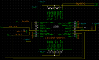
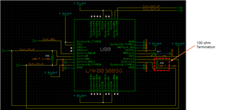
Please see the attached file for detailed pictures.

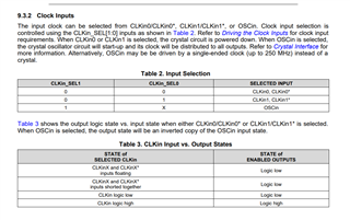
1. I would like to inquire about what happens to the CLOCK output (CLK_OUT_P, CLK_OUT_N) when the CLOCK input line is configured as shown below and input selection is made.

1)Apply the same CLOCK input signal (CLK_IN_P) to CLKin0 and CLKin1*

2)Apply the same CLOCK input signal (CLK_IN_N) to CLKin0* and CLKin1.

Question 1) What is the output signal when CLKin_SEL1=0 & CLKin_SEL0=0?

Question 2) What is the output signal when CLKin_SEL1=0 & CLKin_SEL0=1?

2. Under the same setup conditions as the previous question, what is the difference between having a 100 ohm termination between CLKin1 and CLKin1* and not?

Question about LMK00308.pptx

3. Under the same setup conditions as the previous question, could you test it on EVKIT and let me know the results?

  • Hello Pyungho, 
    There is a selectable input MUX. 

    This table should answer most of your questions. 
    The termination makes no difference, it's to ensure your driver is terminated appropriate.  
    LVDS requires a differential 100Ohm termination. 

    Best regards, 

    Vicente 

  • Thank you for your prompt reply. I am contacting you with additional questions.

    I know that this chip selects and outputs.

    I am curious about what the output will be like when the input signal is split into opposite signals as shown in the figure below.

    I would like to know how to design the circuit

    when the same signal, Positive Clock (CLK_IN_P), is input to CLKin0 and CLKin1*,

    and the same signal, Negative Clock ((CLK_IN_N), is input to CLKin0* and CLKin1.

    Also, when inputting split Clock input, I would like to know whether I should put 100 ohm termination in each input or only in one side.

    Both clock input and output are LVDS.

    I am wondering which is correct between Case 1 and Case 2 when inputting a split Clock.

    Case 1) CLKin0 & CLKin0*: 100 ohm , CLKin1 & CLKin1*: 100 ohm

    Case 2)  only CLKin0 & CLKin0*: 100 ohm

  • Hi Vicente,

    The customer wants to make 2 different clocks; one is in phase and the other one is out of phase.

    In other words, in phase clock output will be generated if CLKin_SEL1=0 & CLKin_SEL0=0 and out of phase clock output will be generated if CLKin_SEL1=0 & CLKin_SEL0=1. Do you think this can be realized properly?

    If it works without any issue, how to terminate CLKin0/0* and CLKin1/1*? Is 100ohm termination needed at each input(2nd figure)? Or only one input(1st figure)?

    Finally, do you have test results regarding this? if not, are you able to test this condition with EVM?

    Best Regards,

    Austin

  • Hi Austin, 
    What is the customer's requirement for having inverted outputs? 
    Why not just have the outputs routed in such a way where you can swap P_N?
    This would ensure not having to worry about glitches due to the IN_SEL MUX changing between the inputs. Any time you switch outputs you will see some glitches as there is usually a settling time given the outputs are asynchronous to the input clocks. 

    This device is not intended for switching on the inputs on the fly as there is no synchronization or gating of the outputs. There will also be some delay due to the power up time for the input buffer when switching over and the internal biasing.

    For glitch less switching of the input reference sources, an alternative device may be the LMK05318 as when this is run in DPLL mode it can provide seamless transitions between reference inputs.

    Best regards, 

    Vicente