This thread has been locked.

If you have a related question, please click the "Ask a related question" button in the top right corner. The newly created question will be automatically linked to this question.

CDCDB800: clock buffer

Part Number: CDCDB800
Other Parts Discussed in Thread: DS320PR1601, LMKDB1108

Tool/software:

Hi,

We are using CDCDB800 clock buffer along with DS320PR1601, in the said clock buffer's datasheet it is mentioned that default termination is 85ohm.

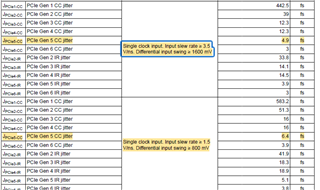
But we are using PCIe Gen 5 Refclk having 100ohm differential impedance.

In clock buffer's datasheet it is specified that we can change the impedance from 85ohm to 100ohm(OUTSET register, bit5).

In section 6.5(Electrical characterstics) it is specified that Zdiff by default is 85ohm but it can be set to 100ohm by setting the respective bit to 1 in OUTSET register.

But this has to be programmed each time when we turn ON the unit, which is practically impossible.

How  can we overcome this scenario?

Thanks and Regards,

Shekha Shoukath

  • Hello Shoukath, 
    Instead of CDCDB00 use LMKDB1108. 

    We have different OPNs, one with Rout being 85Ohm the other option being 1000Ohm differential. 

    It's also p2p with CDCB800. 

    Best regards, 

    Vicente 

  • Hi,

    CDCDB00 is 48 pin but LMKDB1108 is 40pinfootprint will not be same.

    Can we have any other option to make CDCDB00's refclock to 100ohm.

    Thanks and Regards,

    Shekha Shoukath

  • Hi Shekha, 
    You're correct, sorry not p2p. 


    Is there any reason you would not want to use LMKDB1108? Especially given the smaller footprint. 

    The only option would be to make a custom part for you where the impedance by default is set to the 100Ohm option. This would eliminate the need to have to program the impedance selection bit. This custom spin component path can be pursued if business needs require so. 


    Best regards ,

    Vicente 

  • Hi,

    in page no:30 of LMKDB1108 datasheet it is specified that all three modes are required.

    kindly explain .

    Also is it okay if we use 85ohm parallel termination at output of clock buffer (CDCDB800).

    usually pcie refclk is 100ohm, why 85 ohm preferred?

    Thanks and Regards,

    Shekha Shoukath

  • Hi Shekha, 
    What the snippet is reffering to is all OE states should match. 
    For example, say OE is pulled high to disable the output but OE register is enabling the outputs, the output state will still be disabled as all modes are required to be set to enable an output. 

    Some use cases require 85OH especially for interop. 

    lso is it okay if we use 85ohm parallel termination at output of clock buffer (CDCDB800).

    I don't understand what you mean here, you don't need to have a termination as it's controlled via register and is internal to the part? 


    Best regards, 

    Vicente 

  • Hi,

    (a)

     in LMKDB1108's datasheet default value of OE register is not mentioned.

    pins 14,19,30,34 have dual functionality (OE/ SBI), in order to use OE functionality SBI_EN (pin 11) has to be low.

    but then SBI functionality is disabled then how SBI mode, SM bus mode and OE mode is enabled in order to use 8 output clocks.

    in section 8.3.3.3, it is mentioned that all 3 modes has to be enabled, also in section 8.3.2.2 it is mentioned that outputs are enabled without any glitch (assuming register OE and SBI OE are active).

    (b) 

    in section 6.5, under electrical characteristics as per the below the image two jitter values specified foe PCIe 5 common clock:

    under what conditions slew rate become 3.5V/ns and1.5V/ns

    (c)

    in the above images different jitter values are specified.

    what is the actual jitter value of LMKDB1108?

    (d)

    what is the function of SBI mask register?

    if sbi mode enabled what all registers will it use?

    (e)

    in the case of slew rate selection pin, only high specifies fast slew rate and low specifies slow slew rate .

    what are the values for fast and slow slew rate.?

    (f)

    automatic output disable bit is enabled in default state, does this mean if the DUT doesn't receive valid clock input no output clock will be generated?

    Thanks and Regards,

    Shekha Shoukath