This thread has been locked.

If you have a related question, please click the "Ask a related question" button in the top right corner. The newly created question will be automatically linked to this question.

LMK5B33216: I2C communication problem

Part Number: LMK5B33216

Tool/software:

I am currently using I2C to communicate with the LMK5B33216 and have observed the following behavior:

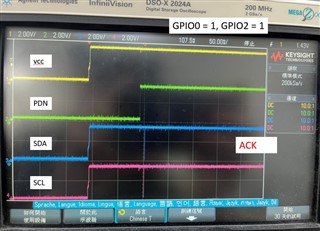
  1. When GPIO0 = 1 and GPIO2 = 1, I2C communication works properly and the signals are stable.

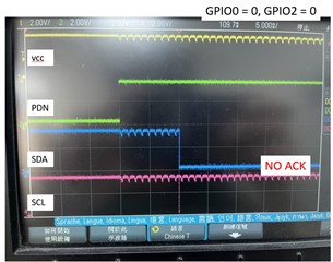
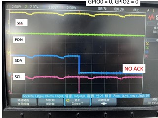
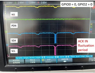
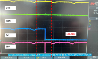
  2. When GPIO0 = 0 and GPIO2 = 0, I2C communication becomes unstable (ACK is not received), and there is slight fluctuation on the VCC line.

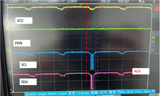
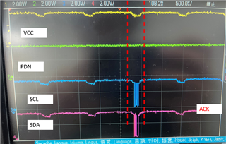
Additionally, I noticed that during the fluctuation period, it is sometimes possible to receive an ACK when I2C signals are transmitted.

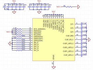
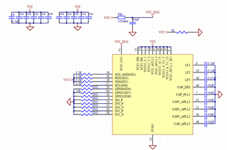
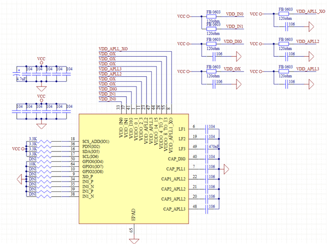
Below is my circuit diagram. I would like to know how to achieve stable I2C communication even when GPIO0 = 0 and GPIO2 = 0.

  • Hi Harry,

    Please allow us time to review. We will get back to you early next week after the US holidays for 4th of July.

    Regards,
    Jennifer

  • Hello Harry,

    The issue appears to be related to the power supply being the same and not isolated for both the analog and digital signals.

    On the schematic it shows that all of the digital signals like I2C clock signals SDA , SCL and VDD_DIG are connected to the same power supply (VCC) as the analog pins. Since the lines are connected to each other, when the analog or digital lines are changing in power this can affect the signal quality of the power supply.

    We can observe this from your images you provided.


    First lets clarify what the two different GPIO settings are. When GPIO0 = 1 and GPIO2 = 1 then the device is set to operate in low power mode so the PLLs of the device are turned off. The PLLs are the analog portion of the device controlling and setting the output frequency.


    Next when GPIO0 = 0 and GPIO2 = 0 the PLLs are turned on and the device is set to operate under normal conditions.

    In the first image provided that shows when GPIO0 = 1 and GPIO2 = 1 we see stable signals. This makes sense because while the PLLs are turned off, there are no analog outputs that can cause corruption on our input signal. This is essentially isolating our digital signals because the analog output portion of the device is not turned on.

    For the other images you provided while the PLLs are turned on we can see a ripple on our power source VCC. This makes sense as now our output frequencies are interfering with our power source and also affecting the digital signals.

    The best way to fix this issue would be to add Ferrite beads to isolate the different power lines in your system.

    For an optimized and reduced supply filtering network you should add a 220 ohm ferrite bead and a 10 uF capacitor close to VDD_DIG pins. 
    If you are planning on generating multiple different output frequencies on multiple different channels you should ask add ferrite beads and capacitors to each output power supply as well.

    Attached below is an image depicting our power filtering from a section of our LMK5B33216 Evaluation Module datasheet.


  • Hi Kyle and Jennifer,

    Thank you for your response. Since I didn’t have any 220 Ω ferrite beads on hand, I substituted with 120 Ω beads and connected VDD_DIG through a 120 Ω bead and a 10 µF capacitor, but the issue persists. In that case, do I need to isolate each VCC rail and add ferrite beads to them individually?

  • Hello Harry,

    A 220 Ω ferrite bead is the most optimal so there may be more noise if you only use a 120 Ω ferrite bead but it should be ok.

    It would be best to use ferrite beads on each of the VCC rails.

    Would you also be able to provide the schematic to review other potential causes of noise?

    Best Regards,
    Kyle Yamabe

  • Hi Kyle,

    Here’s my current schematic. Since modifying our PCB is quite cumbersome, I’d like to ask if there’s any way to pinpoint which VCC pin is causing the issue—or if some configuration isn’t set correctly, leading to the IC’s abnormal startup. It’s also rather odd that communication works intermittently during the voltage oscillations.

  • Hi Kyle,

    I conducted an additional experiment by connecting VDD_DLG externally to VCC2. As a result, I observed the following phenomenon: VCC was pulled down slightly, and the SDA line was pulled to a low level and became unusable.

    GPIO0 = 0;GPIO2 =0

  • Hello Harry,

    Based on the last image that does seem to be the issue with the board. It is possible that other VCC rails could be causing issues as well. 

    The best way to test the other VCC rails would be by testing the board using the GPIO0 = 0 and GPIO2 = 0 configuration and seeing if the voltage rails are affected.

    Since the different sources of interference could be coming from any of the APLLs and Outputs and we are only able to load the configuration on startup I cannot think of another way to test. You would need to program the part to a specific configuration to be able to narrow down if a certain output VDDO or APLL_VDO is causing the issue but since we are limited to loading certain ROMs on startup it we cannot narrow this down with this method.

    Best Regards,
    Kyle Yamabe

  • Hi Kyle,

    Thank you for your reply. I have an additional question.

    The image shows the initial circuit communication. It appears that communication is unstable at first, but within a certain range where VCC is slightly pulled down, communication becomes stable and ACKs can be received normally. Outside of this range, communication fails.

    It seems that the IC enters some kind of communicable mode under these specific conditions. Based on this behavior, is it possible to deduce which pin might be causing the issue, or whether the circuit configuration needs to be modified?

  • Hello Harry,

    You will need to separate power rails for all of the core power supplies all VDD. 

    The can leave the VDDO power rails all together.

    Best Regards,
    Kyle Yamabe

  • Hi Kyle,

    Thank you for your reply. 

    I will modify my circuit to separate the VDD power rail and combine the VDDO lines together, as shown in the diagram below. I would like to ask you the following:

    1. Are there any pins that need to be reserved or any modifications that should be made? If so, please let me know.

    2. Do you have any recommended ferrite bead models? We are planning to proceed with the procurement.

    Thank you!

  • Hello Harry,

    This is our recommended ferrite bead BLM18SG221TN1D.
    Would you be able to provide the layout of your board as well. Some possible other issues that could be causing issues with noise coupling could be the location and proximity of a switching power supply being placed close to the chip. Or other issues like isolated grounds or sharp layout corners causing antennas.

    Adding separate power rails will help but there are still other possible reasons for coupling that could be causing the issue on the power rails.

    Since as you discussed it takes an effort to redesign it would also be good to observe the entire system level layout just in case.

    Best Regards,
    Kyle Yamabe

  • Hi Kyle,

    Since the PCB layout information is relatively confidential, could you please provide your email address so that we can send it to you once the new PCB layout is completed?

    Thank you!

  • Hello Harry,

    I will reach out to you over email.

    Best Regards,
    Kyle Yamabe