


Part Number: LMKDB1108
Tool/software:
Hi,
(a)
in LMKDB1108's datasheet default value of OE register is not mentioned.
pins 14,19,30,34 have dual functionality (OE/ SBI), in order to use OE functionality SBI_EN (pin 11) has to be low.
but then SBI functionality is disabled then how SBI mode, SM bus mode and OE mode is enabled in order to use 8 output clocks.
in section 8.3.3.3, it is mentioned that all 3 modes has to be enabled, also in section 8.3.2.2 it is mentioned that outputs are enabled without any glitch (assuming register OE and SBI OE are active).
(b)
in section 6.5, under electrical characteristics as per the below the image two jitter values specified foe PCIe 5 common clock:
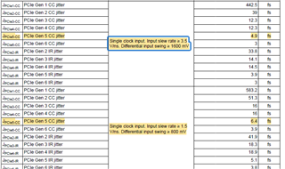
under what conditions slew rate become 3.5V/ns and1.5V/ns
(c)
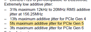
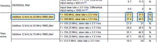
in the above images different jitter values are specified.
what is the actual jitter value of LMKDB1108?
(d)
what is the function of SBI mask register?
if sbi mode enabled what all registers will it use?
(e)
in the case of slew rate selection pin, only high specifies fast slew rate and low specifies slow slew rate .
what are the values for fast and slow slew rate.?
(f)
automatic output disable bit is enabled in default state, does this mean if the DUT doesn't receive valid clock input no output clock will be generated?
Thanks and Regards,
Shekha Shoukath
