This thread has been locked.

If you have a related question, please click the "Ask a related question" button in the top right corner. The newly created question will be automatically linked to this question.

LMK05318: Sync E Hardware connections understanding and Reference

Part Number: LMK05318
Other Parts Discussed in Thread: DP83869HM, , LMK5B12212, LMK5B33414, LMK5B33216, , , AM625, AM6252

Tool/software:

HI TI Team,

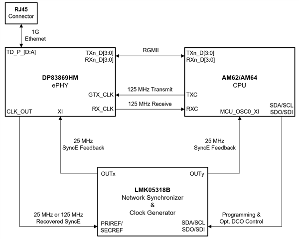
We are looking to interface the AM62x processor with the DP83869HM Ethernet PHY for a 1Gbps Ethernet connection. In addition to that, we want to add Sync E support to our system to connect multiple systems. For this purpose, we are looking to use the Network Synchronizer Clock LMK05318. 

To achieve this and make the first time right design, we are looking for your support regarding the required Hardware connections of all three components altogether. I already referred to this link, but not able to get total clarity on how the connections will be done and communication will take place.

Could you please share the reference design of the Sync E implemented system, if available?
If not available, kindly guide us on how connections will be made.

Thanks & Regards,
Sahil Nayak

  • Hi Sahil ,

    I support the clocking components and specialize in network synchronizers.

    1. Can you please provide insight on the end application?
    2. We recommend using the LMK05318B as that is the latest silicon version. For improved jitter performance, there is also the LMK5B33216 family (LMK5B33414, LMK5B12212) which can be used as well for the SyncE applications.
    3. Will you require use of IEE1588 PTP or 1PPS locking?
    4. We have some general collateral available here on SyncE or SyncE + PTP use case:
      1. https://www.ti.com/product/LMK05318B#tech-docs
      2. https://www.ti.com/product/LMK5B33216#tech-docs
      3. Here is a general block diagram of how the setup can look like for SyncE + PTP:

    Let me know if you need further help.

    Regards,

    Jennifer

  • Hi Jennifer,


    Thank you for your quick response.

    The end application is a data acquisition system.
    Use of IEE1588 PTP or 1PPS locking is TBD as of now.

    I am trying to map the general block diagram with Figure 3 Frequency Synchronization Using the LMK05318 mentioned in this link and I have the following queries:

    • Could you please give more details what does "link" refer to in Figure 3 Frequency Synchronization Using the LMK05318?
    • Sync E feedback clock will be 25MHz. Please confirm.
    • Where will the Sync E clock and Sync E + PTP clock connect?


    Also, I am trying to map the general diagram at the pinout level to get a better understanding of our connections and want to confirm my knowledge on the below-mentioned points:

    • Which pin from LMK05318B will be connected as Sync E feedback clock to which pin of DP83869HM?
    • Which pins will be connected for Sync E recovered clock?
    • The clock inputs and outputs for LMK05318B are differential as per pinout. However, we will have single ended input and output as per my understanding. In that case, can we connect the negative pin of the differential pair to GND or keep it NC?
    • Which oscillator is recommended to be used for LMK05318B input? TCXO or OCXO?
    • Since we are already using netwrok synchronizer, what is the additional advantage of using IEEE1588 PTP/ 1PPS locking? It would be great if you could throw some light on it.
    • I see in the datasheet of the LMK05318B that different types of input and output clocks are supported. Do we need to take care of anything there?


    I am looking for pin-level interface details among the processor, PHY and network synchronizer. It would be great if you can provide this, which helps us to design the same.

    Thanks & Regards,
    Sahil Nayak

  • Hi Sahil,

    1. I did not write the document and it is a bit older. I'm not sure exactly what the writer intended with "link" in that diagram. However, I believe they intended to show a generalized connection (not a real wired connection) between the PHY and the network synchronizer which represents a "link" between the two devices.
    2. Yes, SyncE is typically 25 MHz or 156.25 MHz.
    3. SyncE connects to a reference clock pin (PRIREF or SECREF). For 1588 PTP, there isn't a recovered clock fed into the PRIREF or SECREF pin. Instead, the PTP is applied to make the DPLL DCO corrections which is either pin (GPIO2 and STATUS1) or software controlled. Please refer to the datasheet for more details on this.
    4. Refer to #3 and the LMK05318B generates the clock for the DP83869HM. In the DP83869HM datasheet that the XI pin is a 25 MHz input.
    5. Please refer to the LMK05318B-Q1 datasheet for recommendations on single-ended pin setup:
    6. The TCXO or OCXO decision depends on your holdover requirements. For most SyncE applications, a TCXO is sufficient.
    7. Sure, the app note you linked helps summarize why use SyncE + PTP:
      1. SyncE provides the frequency synchornization whereas IEEE 1588 PTP provides the time/phase synchronization. The PTP phase typically comes from a grandmaster or GNSS clock which is highly accurate. This phase information is transferred between nodes and interpreted by the PTP stack within the logic device such as the FPGA or ASIC. The logic device then sends out the necessary phase adjustments (I2C/SPI or GPIO control) to the LMK05318B device to correct the phase of the network synchronizer. PTP is used where you want to maintain precise timing in your network. If precise timing is not required, then "SyncE only" can be sufficient where keeping the same phase domain does not matter and all that matters is maintaining the same frequency domain.
    8. "Do we need to take care of anything there?"
      1. Can you please clarify your question? The input and output is dependent on the input driver and the output receiver specifications. For example, DP83869HM states in the datasheet that the 25 MHz single-ended input is required. This means an LMK05318B LVCMOS output is necessary for the input of the DP83869HM .
    9. "I am looking for pin-level interface details among the processor, PHY and network synchronizer. It would be great if you can provide this, which helps us to design the same."
      1. We do not have such level of detail at this time. If you have further questions while you work on designing, please continue to make e2e posts. I suggest you look at the EVM schematics from each device to help you get a better idea.

    Regards,

    Jennifer

  • Hi Jennifer,

    Thank you for your detailed response.

    Please find my response inline below:

    1. I did not write the document and it is a bit older. I'm not sure exactly what the writer intended with "link" in that diagram. However, I believe they intended to show a generalized connection (not a real wired connection) between the PHY and the network synchronizer which represents a "link" between the two devices.

    [Sahil]: Understood.

    1. Yes, SyncE is typically 25 MHz or 156.25 MHz.

    [Sahil]: Understood. How is the SyncE frequency decided?

    1. SyncE connects to a reference clock pin (PRIREF or SECREF). For 1588 PTP, there isn't a recovered clock fed into the PRIREF or SECREF pin. Instead, the PTP is applied to make the DPLL DCO corrections which is either pin (GPIO2 and STATUS1) or software controlled. Please refer to the datasheet for more details on this.

    [Sahil]: We are looking to implement SyncE and don't require very precise timing. So, I think we don't need PTP. In case we need to add PTP support, are there any Hardware connections required, or is it totally implemented by software? Please confirm my understanding.

    1. Refer to #3 and the LMK05318B generates the clock for the DP83869HM. In the DP83869HM datasheet that the XI pin is a 25 MHz input.
    1. Please refer to the LMK05318B-Q1 datasheet for recommendations on single-ended pin setup:

    [Sahil]: Does the same logic apply for output differential clocks as well?

    1. The TCXO or OCXO decision depends on your holdover requirements. For most SyncE applications, a TCXO is sufficient.

    [Sahil]: Understood. What are the tolerance requirements for selection of TCXO?

    1. Sure, the app note you linked helps summarize why use SyncE + PTP:
      1. SyncE provides the frequency synchornization whereas IEEE 1588 PTP provides the time/phase synchronization. The PTP phase typically comes from a grandmaster or GNSS clock which is highly accurate. This phase information is transferred between nodes and interpreted by the PTP stack within the logic device such as the FPGA or ASIC. The logic device then sends out the necessary phase adjustments (I2C/SPI or GPIO control) to the LMK05318B device to correct the phase of the network synchronizer. PTP is used where you want to maintain precise timing in your network. If precise timing is not required, then "SyncE only" can be sufficient where keeping the same phase domain does not matter and all that matters is maintaining the same frequency domain.
    2. "Do we need to take care of anything there?"
      1. Can you please clarify your question? The input and output is dependent on the input driver and the output receiver specifications. For example, DP83869HM states in the datasheet that the 25 MHz single-ended input is required. This means an LMK05318B LVCMOS output is necessary for the input of the DP83869HM .
    3. "I am looking for pin-level interface details among the processor, PHY and network synchronizer. It would be great if you can provide this, which helps us to design the same."
      1. We do not have such level of detail at this time. If you have further questions while you work on designing, please continue to make e2e posts. I suggest you look at the EVM schematics from each device to help you get a better idea.

    [Sahil]: Please share schematic links to the EVMs.

    In addition to this, I have attached a pin-level SyncE block diagram of the connections required to be done for SyncE. We will have 2x RJ45 ports on our board and want to implement SyncE. Kindly review the connections and let me know if this is correct or anything else needs to be added.

    Thanks & Regards,
    Sahil Nayak

    SyncE Block Diagram.pdf

  • Hi Sahil,

    1. SyncE frequency is decided by the application needs or receiver/driver requirements. For example, the DP83869HM receives a 25 MHz (SyncE) clock and no other frequency so you must pick 25 MHz as the output frequency.
    2. Regarding using PTP later, if you prefer to make the DCO adjustments by software, then GPIO control is not necessary and you only need to ensure the I2C/SPI bus is connected to the host device and that a feedback close is routed back to the host so the PTP stack knows how much correction to make.
    3. "Does the same logic apply for output differential clocks as well?"
      1. For differential clocks, please refer to the 9.3.12 Clock Outputs (OUTx_P/N) and 9.3.14 Clock Output Interfacing and Termination sections.
    4. "What are the tolerance requirements for selection of TCXO?"
      1. Please refer to the SyncE spec (such as ITU-T G.8262) which specifies an accuracy of 4.6 ppm. This means the TCXO and PRIREF/SECREF inputs should not deviate beyond the 4.6 ppm. The accuracy of the network synchronizer outputs depends on the PRIREF/SECREF input when the DPLL is locked and the XO/TCXO/OCXO input when the DPLL is unlocked.
    5. You may find the schematics available on each product page in the Technical Documentation or Design & Development sections.
      1. https://www.ti.com/lit/pdf/snau253
      2. https://www.ti.com/product/DP83869HM#design-development  and https://www.ti.com/lit/pdf/snlu237
      3. https://www.ti.com/tool/SK-AM62B-P1#design-files

    Regards,

    Jennifer

  • Hi Jennifer,

    Thank you for the details.

    Did you get a chance to review the connection block diagram that I attached in my previous response?
    Attaching here again for your reference. 

    8802.SyncE Block Diagram.pdf

  • Oh right, I meant to ask if you could please export the PDF in "landscape" mode. It is a bit hard to follow as two pages (cropped).

    Thank you,

    Jennifer

  • Hi Jennifer,

    Please see the attached connection block diagram PDF.

    SyncE Block Diagram.drawio.pdf

  • Hi Sahil,

    Thank you, the diagram is much better. Please allow me a few days to review and confirm the connections with the other teams (ePHY and CPU, I'm only the clocking side for LMK05318B). I'll reach back early next week.

    Regards,

    Jennifer

  • Hi Jennifer,

    Sure, thanks for the update.

    Thanks & Regards,
    Sahil Nayak

  • Hi Sahil,

    Question for you, what part number did you plan to use for the AM62x? Was it AM625?

    Regards,

    Jennifer

  • Hi Jennifer,

    We are planning to use the AM6252/AM6254 processor.

  • Hi Sahil,

    You had most of it correct except for the RXC clock routing which should be between the CPU and the ePHY.

    1. The ePHY has a dedicated CLK_OUT pin for the SyncE recovered clock, which should then be used to feed into the network synchronizer. More details on setting the CLK_OUT pin:
      1. By default, CLK_OUT is buffered to XI input clock. You'd need to change the register to make CLK_OUT source from the recovered (SyncE) clock, see Section 7.3.3 Clock Output.
      2.  [FAQ] DP83869HM: How to generate 125MHz on CLKOUT pin for DP83869 
    2. Also, I recommend looking at these AM62 design files which contains the full schematic and block diagrams of how to connect between the CPU and ePHY.
      1. https://www.ti.com/tool/SK-AM62B-P1#design-files

    Regards,

    Jennifer

  • Hi Jennifer,

    Thank you for your confirmation and suggestions.

    1. Regarding Point #1, if we want a 1Gbps speed, what should be the frequency of the recovered clock? 25MHz or 125MHz?

    2. Also, in the block diagram you attached, I can see a connection between the OUTy pin of the Network Synchronizer and the XI pin of the processor (25MHz of SyncE feedback). Could you please explain the significance of this connection? And what does the XI pin of the processor refer to?

    Thanks & Regards,
    Sahil Nayak

  • Hi Sahil,

    1. I am double checking this with the ePHY team. From my understanding, it shouldn't matter if 25 MHz or 125 MHz is used because the recovered SyncE clock is transferring frequency information, that is, the frequency accuracy. The same frequency accuracy can be conveyed whether it's 25 MHz or 125 MHz.
    2. Ah, I meant to put "MCU_OSC0_XI". Here is the corrected diagram:

    Regards,

    Jennifer

  • I confirm that from the PHY perspective, 25 MHz or 125 MHz to the network synchronizer does not matter. What matters is that the input frequency to the synchronizer is a SyncE recovered clock source and that the synchronizer generates 25 MHz as the frequency for the PHY's clock input (XI).

  • Hi Jennifer,

    Noted. Thank you for the details.

    Lastly, please confirm the updated block diagram. I have updated it as per your recommendations.
    Let me know if still something is missing.

    Thanks & Regards,
    Sahil Nayak

    SyncE Block Diagram-Updated.pdf

  • Hi Sahil,

    This looks good to me.

    Regards,

    Jennifer

  • Hi Jennifer,

    Thank you for your confirmation and support.

    Once the schematic is ready, I will post a new thread for its review.

    Thanks & Regards,
    Sahil Nayak

  • Hi Jennifer,

    I have one additional query.

    As per the SyncE block diagram that I shared, OUT6_P of the Network Synchronizer will connect to the XI pin of the PHY. We want it to operate on 3.3V since we will be operating the PHY on 3.3V. So, will it be possible to generate a 3.3V LVCMOS clock on the OUT6_P?

  • Hi Sahil,

    You bring up a good point and are right to check the swing spec between the LMK05318B and DP83869HM .

    The LMK05318B LVCMOS output swing is recommended for 1.8V (VDDO = 1.8V) due to the internal drop out voltage.

    From LMK05318B datasheet:

    However, from the DP83869HM datasheet, we see that a minimum swing of 1.2V is required for XI VIH, which means the 1.8V LVCMOS output from LMK05318B is OK.

    Regards,

    Jennifer