This thread has been locked.

If you have a related question, please click the "Ask a related question" button in the top right corner. The newly created question will be automatically linked to this question.

[FAQ] TLC555: What are the performance differences expected for TLC555 PCN 20231130002.1?

Part Number: TLC555
Other Parts Discussed in Thread: , TLC3555-Q1, TLC3555

Tool/software:

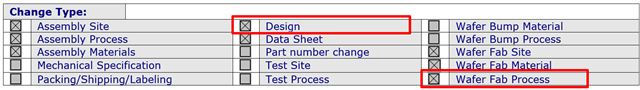
PCN 20231130002.1 is the “Qualification of RFAB using qualified Process Technology, Die Revision, Datasheet update and additional Assembly Site/BOM options for select devices”. Devices affected are TLC555C, TLC555I, TLC555Q, but not TLC555-Q1.

What are the performance differences expected?

  • The key changes are Design and Wafer Fab Process; this means changes to device schematic and the components used. This is a major change. These changes make the part better. This is beneficial for new designs and may be troublesome for old designs where the key care about is being the consistently same.

    This is a list of things that are better POST-PCN; in the order that better likely has negative ramifications in applications.

    1. Lower propagation delays, make results closer to design simple formulas
    2. Improved ESD performance
    3. Startup circuit added for more reliable start up
    4. Fixed the flaw where THRES can override TRIG, when CONT is less than 2/3 VDD.
    5. Reset pin has internal pull up; allows floating RESET pin.
    6. CONT pin resistive divider changes FET to resistors
    7. Faster rise and fall time

    These are the natural and unexpected side effects of POST-PCN being better

    1. A-stable oscillator will have a higher output frequency
    2. Internal diode on DISCH to VDD prevents having DISCH voltage greater than VDD
    3. VDD glitches can upset timing waveform output
    4. Some applications depend on the flawed truth table operation
    5. Reset used with RC networks will ramp differently due to 860k internal pull up
    6. Slightly different CONT pin charge up time with capacitor
    7. More EMI on poorly laid out circuit boards

    Other differences

    1. Power off pin curves are different which could affect some in circuit production testing
    2. Output when RESET crosses threshold could oscillate at high frequency.
    3. VOL and VOH curves lower on resistance
  • Bullet #1, Lower propagation delays so a-stable oscillator will have a higher output frequency

    This chart shows how much faster the post PCN should be based on the original PRE-PCN observed frequency. Supply voltage affects the amount of frequency increase. Lower supply voltage will have more change. There is little frequency increase at 1kHz and substantial increase when original frequency is over 100kHz.

    Note that Ideal a-stable frequency is based on these simple low and high time formulas. Frequency is 1/(tH+tL). 

    The ideal formula does not include propagation delay (tPLH, tPHL) which causes ramp voltage to be larger. A more accurate formula is below. Frequency is 1/(tC(H)+tC(L)). 

    The PCN reduces propagation delay so frequency will be faster but still lower than ideal formula. Use table below for delay based on supply voltage. For voltage between 3V and 5V interpolate based on 3V and 5V entries. For voltage between 5V and 15V interpolate based on 5V and 15V entries.

    PRE-PCN

    tPD LH

    tPD HL

    3V

    320 ns

    250 ns

    5V

    250 ns

    200 ns

    15V

    160 ns

    160ns


    POST-PCN

    tPD LH

    tPD HL

    3V

    88 ns

    74 ns

    5V

    80 ns

    67 ns

    15V

    56 ns

    47ns

  • Bullet #2, Improved ESD performance

    A diode was added internally from pin 7, DISCH to pin 8, VDD. This helps with ESD but it can affect applications where DISCH voltage can exceed VDD. The pin 7 power off curve sweep vs pins 1 and 8 (GND & VDD) shows the added diode.

  • Bullet #3, Startup circuit added for more reliable start up

    Pre PCN TLC555 didn’t have start up circuit. It started up naturally. In rare cases, the bias circuity does not power up. Post PCN added a start up circuit to ensure proper startup under all process and temperature extremes.

    However large amplitude and fast slew rate VDD glitches can cause POST-PCN to change the output state unexpectedly. Pre-PCN is not affected. The data sheet is clear that proper bypass capacitance is required. If this advice is followed then no large or fast VDD glitches should occur. Glitches above the line (larger or faster slew rate) can cause improper output signals.

  • Bullet #4, The PCN fixed the flaw where THRES can override TRIG

    Only a few applications apply TRIG and THRES at the same time while forcing CONT to low voltage. These applications can have a different output state because PRE-PCN has a truth table flaw and POST-PCN does not have this flaw.

    Applications that depend on this flaw will no longer work the same. In the chart, TRIG is low and THRES is high, both active. Per truth table TRIG should override THRES making output high. When CONT voltage is low then output may be low in conflict with truth table.

    The hysteresis in the chart data is an area where output could be high or low depending on sequence or applying TRIG and THRES at same time and CONT being lower voltage.  

  • Bullet #5, Reset pin has internal pull up; this allows floating RESET pin

    An 860kΩ nominal value pullup resistor was added from pin 4 to pin 8. Over the temperature range -40C to 125C, resistance can change -6% to +18%. Pre-PCN pin RESET input is high impedance.

  • Bullet #6, CONT pin resistive divider changes FET to resistors

    Pre-PCN design used matched FETS to make the 3R internal resistor divider. The ratios were good, but the impedance at CONT pin varied considerably across supply voltage and temperature (sloped curves). Post-PCN uses resistors for the 3R divider, so CONT pin impedance is more stable across supply voltage and temperature (flatter curves)

  • Bullet #7, Faster rise and fall time

    Output pin should be treated as a logic signal for EMI purposes in board layout.

    FALL

    PRE

    POST

    5V

    7.9 ns

    1.8 ns

    15V

    5.3 ns

    2.6 ns


    RISE

    PRE

    POST

    5V

    12.2 ns

    3.7 ns

    15V

    7.9 ns

    4.0 ns

  • Bullet #8, Power off pin curves are different which could affect production in-circuit-testing

    Curve sweeps for VDD = 0V have changed with the PCN.

    Pins 2, 4, 5, 6 remove the resistance from PIN to PIN 8 (VDD) internal current

    Pins 3 and pin 8 are similar for PRE and POST PCN. Note pin 8 is to GND only

    Pins 7 has an added diode to pin 8 in Post-PCN design


  • Bullet #9, Output when RESET crosses threshold could oscillate at high frequency (super MHz) with higher quiescent current.

    This occurs when TRIG is active low and RESET voltage is rising. When TRIG is inactive high or when RESET voltage is falling, this issue does not occur. Below is slow ramping (2 seconds per division) RESET voltage and VOUT versus time. 


  • Bullet #10, VOL and VOH curves have lower on resistance

    Charts represent VDD = 5V data. The lower on resistance should not affect application performance unless output becomes shorted. Short current will be higher.

  • Short term solutions to restore previous application results 

    TLC555-Q1 can be used as a replacement orderable for SOIC package. It is immune from this first PCN. It runs with VDD as low as 2V but the specifications in data sheet are 5V minimum. A future 2nd PCN will replace all TLC555 including TLC555-Q1; it will be a close to original device replacement but not exact. The threshold override trigger flaw will not be in the 2nd PCN.

    Longer term solutions to maintain proper application results.

    TLC3555-Q1 can be used after external components are tuned for TLC3555-Q1 performance. TLC3555-Q1 has no design/process PCN so it is always (to date) the same process and design. TLC3555-Q1 will not work when DISCH > VDD or THRES should override TRIG flaw is needed. A future commercial grade TLC3555 will be released with identical typical performance as TLC3555-Q1 but without automotive qualification.