Other Parts Discussed in Thread: LMK04616
Tool/software:
Hi team,
i'm using the clock distributor LMK04610 for a new project.
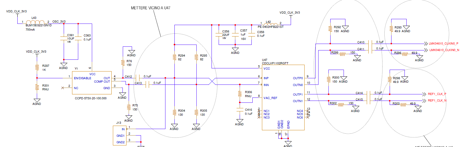
In the following picture there is the electrical schematic that i devoloped for the reference clock distribution from the LVPECL 100 MHz oscillator to LMK04610:
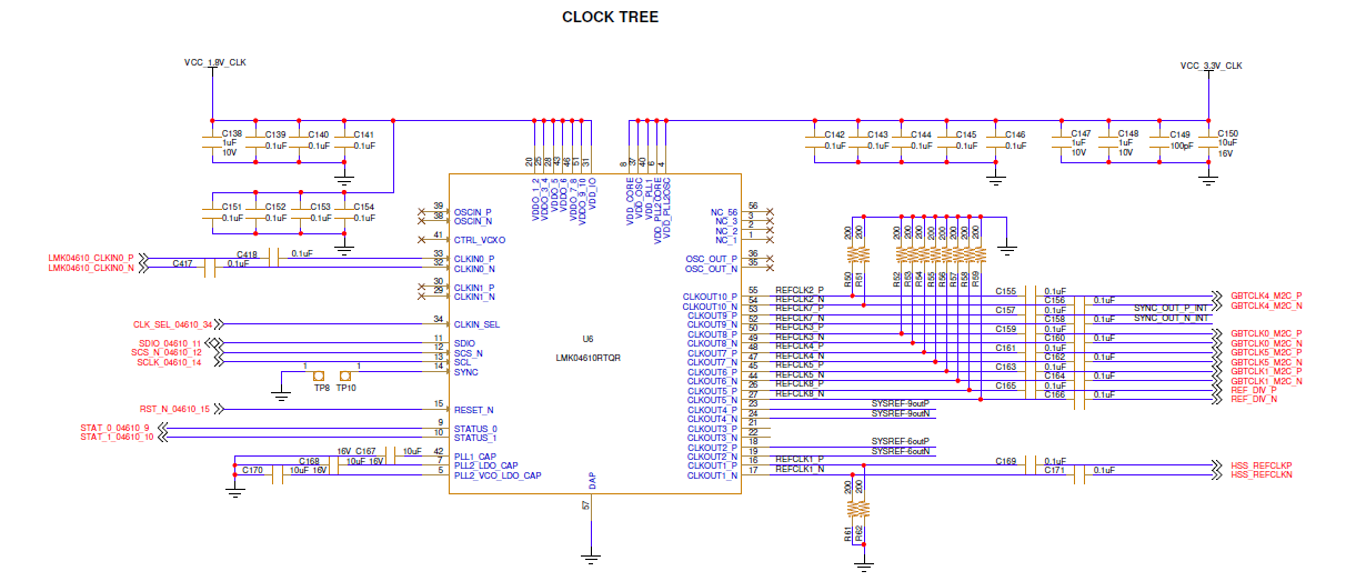
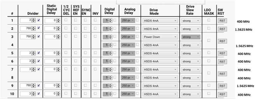
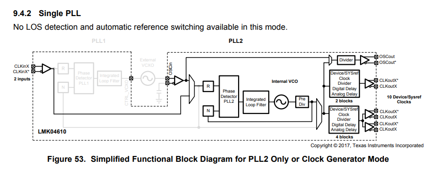
In particular, the LMK04610 must work in single PLL mode (PLL1 bypass and no external VCXO):
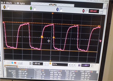
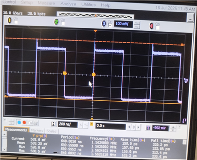
From the 100 MHz LVPECL input, the outputs are at 400 MHz for the CLKOUT10,CLKOUT8, CLKOUT7, CLKOUT6, CLKOUT5 and CLKOUT1. The CLKOUT2, CLKOUT4 and CLKOUT9 are at 1.5625 MHz.
I tried this configuration through the relative evaluation board and it works correctly.
I attach the configuration file that i downloaded from TICS Pro.
When I try to upload this file to my board, the LMK04610 doesn't work (no frequencies generated).
Why doesn't it work?
Are there any errors in the configuration file?
Are the registers not written in the right order?
Thank you in advance.
Best Regards,
Matteo Ricci
R0	0x000000
R1	0x000100
R2	0x000200
R3	0x000346
R4	0x000438
R5	0x000503
R6	0x00061B
R7	0x000700
R8	0x000800
R9	0x000900
R10	0x000A00
R11	0x000B00
R12	0x000C51
R13	0x000D08
R14	0x000E00
R15	0x000F00
R16	0x00101E
R17	0x001100
R18	0x001204
R19	0x001310
R20	0x001480
R21	0x001508
R22	0x001648
R23	0x001700
R24	0x001800
R25	0x001931
R26	0x001A32
R31	0x001F00
R32	0x002078
R33	0x002100
R34	0x002278
R39	0x002714
R40	0x002808
R41	0x002914
R42	0x002A08
R43	0x002B00
R44	0x002C80
R45	0x002D00
R46	0x002E16
R47	0x002F08
R48	0x003001
R49	0x00310C
R50	0x003200
R51	0x003300
R52	0x003443
R53	0x003510
R54	0x003603
R55	0x003700
R56	0x003843
R57	0x003910
R58	0x003A03
R59	0x003B00
R60	0x003C43
R61	0x003D10
R62	0x003E43
R63	0x003F00
R64	0x004043
R65	0x004110
R66	0x004203
R67	0x004300
R68	0x004403
R69	0x004503
R70	0x004600
R71	0x004703
R72	0x004800
R73	0x004900
R74	0x004A03
R75	0x004B00
R76	0x004C03
R77	0x004D00
R78	0x004E03
R79	0x004F03
R80	0x005000
R81	0x005100
R82	0x005203
R83	0x005300
R84	0x005430
R85	0x005500
R86	0x00560D
R87	0x005718
R88	0x00583F
R89	0x005961
R90	0x005A0A
R91	0x005B02
R92	0x005CCA
R93	0x005D00
R94	0x005E00
R95	0x005F61
R96	0x0060A8
R97	0x006100
R98	0x006278
R99	0x006300
R100	0x006440
R101	0x006500
R102	0x006600
R103	0x006700
R104	0x006800
R105	0x006900
R106	0x006A09
R107	0x006B01
R108	0x006C01
R109	0x006D28
R110	0x006E1F
R111	0x006F03
R112	0x007000
R113	0x007100
R114	0x007214
R115	0x007300
R116	0x007406
R117	0x007500
R118	0x007601
R119	0x007701
R120	0x0078FF
R121	0x007900
R122	0x007A86
R123	0x007BA0
R124	0x007C08
R125	0x007D00
R126	0x007E00
R127	0x007F34
R128	0x00800A
R129	0x008100
R130	0x008200
R131	0x008300
R132	0x00840F
R133	0x008501
R134	0x008601
R135	0x008700
R136	0x008840
R137	0x008900
R138	0x008A00
R139	0x008B40
R140	0x008C00
R141	0x008D00
R142	0x008E00
R143	0x008F40
R144	0x009000
R145	0x009100
R146	0x009280
R147	0x009380
R148	0x009404
R149	0x009500
R150	0x009610
R151	0x009720
R152	0x009820
R153	0x009980
R155	0x009B00
R156	0x009C20
R171	0x00AB00
R172	0x00AC00
R173	0x00AD00
R175	0x00AF00
R176	0x00B001
R190	0x00BE03
R246	0x00F600
R247	0x00F700
R249	0x00F907
R250	0x00FAD7
R252	0x00FC00
R253	0x00FD00
R254	0x00FE00
R255	0x00FF00
R256	0x010000
R257	0x010100
R258	0x010200
R259	0x010300
R260	0x010400
R261	0x010500
R262	0x010600
R263	0x010700
R264	0x010800
R265	0x010900
R266	0x010A00
R267	0x010B00
R269	0x010D00
R270	0x010E00
R272	0x011000
R273	0x011100
R274	0x011200
R277	0x011500
R278	0x011600
R279	0x011700
R281	0x011900
R282	0x011A00
R292	0x012408
R295	0x012704
R296	0x012801
R297	0x012905
R298	0x012A01
R299	0x012B04
R300	0x012C05
R301	0x012D04
R302	0x012E01
R304	0x013005
R305	0x013105
R307	0x013305
R308	0x013405
R309	0x013505
R312	0x013805
R313	0x013905
R314	0x013A05
R316	0x013C05
R317	0x013D05
R320	0x01400A
R321	0x014109
R322	0x014240
R323	0x014300
R325	0x014500
R326	0x01462C
R329	0x014900
R330	0x014A00
R331	0x014B00
R332	0x014C00
R334	0x014E00
R336	0x015000
R337	0x015114
R338	0x01520F
R339	0x015300