This thread has been locked.

If you have a related question, please click the "Ask a related question" button in the top right corner. The newly created question will be automatically linked to this question.

LMK04828: Can't make LMK04828B use CLKIN0

Part Number: LMK04828
Other Parts Discussed in Thread: LMK04832

Tool/software:

Hi,

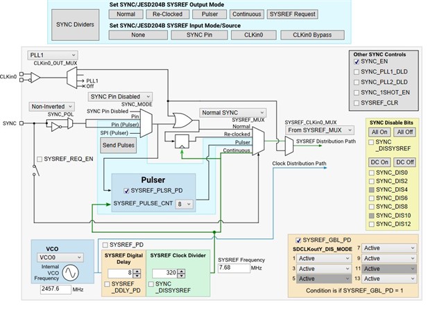
I'm using the CLK104 board on the Xilinx ZCU216 (RFSoC) eval board.  I have been trying for several days to get the CLK104 board (which uses the LMK04828B) to accept a clock input on the SMA connector that feeds into CLKIN0.  No matter what I do, the LMK04828B uses the onboard 10MHz TCXO that is connected to CLKIN1.  I have attached the .tcs file that I am using with TICS PRO.

Also, I'm writing all 136 registers that TICS PRO generates out to the LMK04282.  The Xilinx supplied code (XRFCLK.C) only writes 128 registers.  I believe this is because there are 8 registers that are read-only?

Thanks,

Dan


245M76_PL_122M88_SYSREF_7M68_CLK0.tcs

  • Based on the TCS file, you seem to be doing everything right at the inputs - you have forced manual mode selection of CLKin0, which should in all cases use CLKin0 input buffer as the sole input source, and disabled the mux routing CLKin1 to the PLL.

    How are you determining which clock is being selected? If you read back R388, and review the RB_CLKinX_SEL fields, does it indicate that CLKin1 is being selected, even though you are programming the device to manually select CLKin0?

    If you set HOLDOVER_EN=0, do you see a difference? I don't think this should matter, but it's a quick check.

    Is there an enable pin on the TCXO that can be toggled to force the output off? 10MHz sine wave signals are susceptible to a lot of locking issues due to the inadequate slew rate relative to the required input minimum slew rate (2π*f*Vpk is around 0.1V/ns best case at 10MHz, whereas LMK04828 expects >0.15V/ns), and if you're putting a sine wave 10MHz into CLKin0 and a square wave TCXO into CLKin1, it's possible the crosstalk from CLKin1 is overpowering the slow sine wave on CLKin0 - but I'd expect this configuration would lose lock at a rate proportional to the frequency error between the two sources. This is also very likely to happen if CLKin0 is not connected to anything while the TCXO is still running on the pins right next to it.

    ---

    Incidentally, does this configuration lock? You should set PLL2_N_CAL equal to PLL2_N in this case. The default loop filter with C2 = 3.9nF and R2 = 0.62kΩ at 6.4MHz phase detector frequency is not very high phase margin, either - about 27° - and you might consider swapping the 0.62kΩ with 2.2kΩ for better stability if you plan to operate at 6.4MHz phase detector. I think you could also enable the doubler and cut the PLL2_N and PLL2_N_CAL values in half to operate at 12.8MHz phase detector for 3dB in-band noise improvement.

  • Hi Derek,

    First, I want to thank you for responding so quickly and also to let you know that it will take me a day or two to go through everything that you've outlined.  I will let you know what I find out!

    Thank you again,

    Dan

  • Hi Derek,

    I was able to get the CLKIN0 working once I found a reliable 10MHz source with square wave output.

    I have attached another TICS PRO config file that shows how I am generating 245.76MHz outputs on the clock dividers with a 10MHz clock on CLKIN0.  I am also using Cascaded ZDM.  BTW, I don't really care about the phase relationship between CLKIN0 and the output clocks...I'm just not sure if I need ZDM to sync the outputs.

    We want to have multiple LMK04828B PLL boards all driven by a common clock (10MHz in this case) and also have the 245.76MHz output clocks in phase.

    I've read the Multi-Clock Synchronization App Report (SNAA294-December 2019) but it's still not clear to me how to make this work.

    Can I use the SYNC pin input on the LMK04828B to reset the dividers and guarantee phase alignment of the output clocks across all devices?

    Thank you for your help!

    Dan

    0167.10MHZ_CLKin0_245.76MHZ_out_ZDM_Cascaded.tcs

  • The SYNC pin is implemented in CMOS, and the internals have a lot of propagation delay and variation across temperature - range is nominally 3-5ns. The SYNC pin is re-timed to the clock distribution path, which in this case is running at 2.4576GHz (~400ps period). Since you say you have multiple LMK04828B PLL boards which need their clocks synchronized, and since the SYNC pin retimes to a 400ps VCO with unknown variation in propagation delay between boards, it seems unlikely that the SYNC pin could accomplish what you want.

    CLKin0 can be configured as an alternate divider sync source, and the CLKin0 circuitry is implemented in CML all the way up to the VCO retimer. The propagation delay and variation across PVT are an order of magnitude smaller than the VCO period, making CLKin0 suitable as a SYNC source at high speeds like this.

    If you have a way to reliably send a sync event into CLKin0 within the same 400ps window across multiple boards, then the scheme you've outlined is plausible. I don't think ZDM is needed, since you've already indicated that you don't care about input-to-output phase, just that outputs across all boards are aligned.

    In the likely event that you do not have a way to reliably send a sync event into CLKin0 within the same 400ps window across multiple boards, things get tricky. There is a re-timer in the SYSREF divider which is nominally intended to make this kind of thing easier by opening the window up from one VCO period to one SYSREF divider period. Then, by putting the SYSREF divider in nested ZDM, the phase of the SYSREF divider (and thus the output divider SYNC retimer) can be related to the input reference phase, against which it is usually much easier to coordinate a SYNC event. But with the SYSREF frequency at 0.8MHz and the clock input at 10MHz, the GCD frequency is 0.4MHz, which is a >1 N-divider and a >1 R-divider - even if you took advantage of nested ZDM to establish a known phase relationship between the SYSREF divider and the clock input, the >1 N and R divide values mean that there are two potential phases of the SYSREF divider for each CLKin cycle, and you don't know what the relationship is across systems, so there's no way to use the SYSREF divider retimer reliably. This limitation is fundamental to LMK04828, and unless you can bump the SYSREF frequency down to 0.4MHz to make N = 1 and trivialize the SYSREF to CLKin phase relationship, the best you can do is try to SYNC through CLKin0 against the 400ps window.

    On the other hand, LMK04832 is p2p with LMK04828, has most of the same features (if not improvements on those features) and includes an R-divider sync feature. So by resetting the R-divider and controlling the placement of the R-divider output (and thus the phase detector edge at PLL1), we could guarantee the phase of the N-divider and the SYSREF divider as well. The R-divider sync has a 100ns window (one 10MHz period) to get it right across all systems, which is usually plausible in multi-board systems. And then the SYSREF divider could re-time the output divider sync event across all boards with a 2.5µs timing window, which is certainly doable.

  • Hi Derek,

    Thanks for the quick response.  We are interfacing to a Xilinx (AMD) ZU49DR RFSoC.  One of the requirements is for the Sysref clock input (on the RFSoC)  to be 7.68MHz.  This is a Multi-Tile Sync (MTS) constraint.  So, it won't be possible to change that clock to 0.4MHz.  Also, we're using a ZCU216 Evaluation board for our development and don't have the option to use a different PLL.  However, I believe we could change our input reference clock to 122.88MHz and change the 160MHz VCXO to 122.88MHz as well.  If we make those changes and distribute 122.88MHz to all the boards as the reference input, will the outputs be phase aligned?  Or, would I also need to enable ZDM to make that happen?

    On SYNC/SYSREF settings, I would configure as shown in the attached image?

    Thanks,
    Dan

  • Hi Dan,

    Changing the input reference and the VCXO would ultimately not change the frequency of the clock distribution path (2.4576 GHz), but it would result in improved phase noise performance for the PLLs. 

    Like Derek said above, the simplest course of action would be to use CLKin0 as a SYNC source and CLKin1 as the input for the reference. 

    Thanks,

    Michael

  • Hi Michael,

    Thanks for the reply.  I'm not questioning your expertise on this, but I'm confused how I could ever use the SYNC PIN input on the LMK04828.  The VCO frequency range (as far as I can tell) is going to be in the 2GHZ - 3GHZ range.  So, I'm just not sure how the SYNC PIN could ever be used if the issue is propagation delay on that input?

    Also, we can't make the changes that you and Derek have recommended because we are using a 3rd party board from Xiinx (CLK104 board).  It is not possible to switch the inputs on CLKin0 and CLKin1.  So, I am looking at swapping the LKM04828 with the LMK04832 on those boards.

    Thanks,
    Dan

  • Hi Dan,

    Swapping the LMK04828 for the LMK04832 is the optimal course of action. The larger R Divider SYNC window is better suited for your multi-device system.

    Thanks,

    Michael

  • Hi Michael,

    Thanks for the reply.  Is there an app note somewhere that explains how to do multi-device sync with the LMK04832?

    Dan

  • Hi Dan, 
    Found on the LMK04832 device homepage. Link below :) 
    Synchronization of Multiple LMK0482x Devices


    Best regards, 

    Vicente