This thread has been locked.

If you have a related question, please click the "Ask a related question" button in the top right corner. The newly created question will be automatically linked to this question.

CDCE72010 SPI port programming problem

Other Parts Discussed in Thread: CDCE72010, CDCLVD1208

Hi,

I have used the CDCE72010 GUI app to set up one of these devices on another board and have done so successfully.

I've exported the register state I like from the GUI and used it to program another CDCE72010 in another system, but I don not get any output clocks after doing so.

The 1st system has a TUSB3210 USB port I access through the GUI.

The 2nd system I am using an Aardvark USB/SPI dongle.

I have captured the SPI data streams being written to both systems with a logic analyzer and verified they are in fact identical.

What am I missing that would prevent the chip in the 2nd system from outputting clocks?  I tried a reset but that doesn't seem to make any difference.

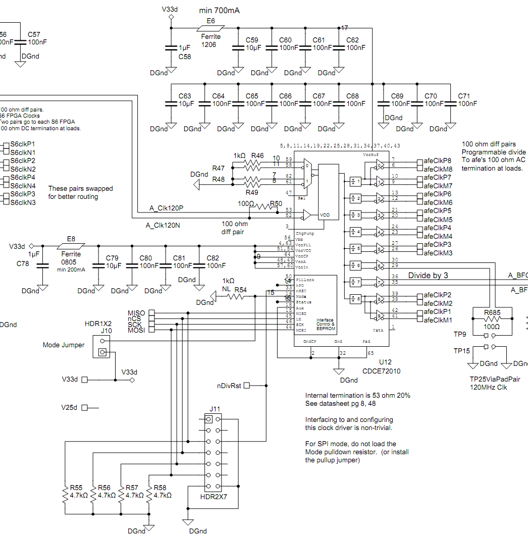
The one difference between the 2 systems is the 1st is driven by an LVCMOS level clock and the 2nd is driven by LVDS.  (I did change the VCXO input to LVDS, external termination, DC)


By the way, why does this chip want SPI data LSB first?  That's a pain.  I have to take all the data from the GUI, mirror it and then re-enter the result in my SPI tool. :-(

Plug: Excalibur free calculator for Windows does a nice job with that.  http://home.comcast.net/~dbernazzani/


Thanks.

  •  

    Here is what my schematic looks like in case you can see anything wrong.

  • Hi David,

    Since the device has no internal VCO, there is not really a calibration routine that could prevent the outputs from turning on and toggling. I suspect the problem you experience has to do with the input signal biasing. Could it be that your input signal is not properly biased to 1.2V? Some LVDS output drivers don't really bias the output signal but expect this to be done on the receiver input. Is there an AC coupling cap by chance between TX output and the CDCE72010 VCXO input? I recommend doing the following things:

    1. Write the exact same settings to device #2 as you have on board #1, and drive an external CMOS signal, just to see if you can replicate proper CMOS operation

    2. After step 1 was successful, verify that you have a common mode voltage of 1.2V for LVDS. If you aren't sure, remove the external 100-Ohm resistor R50 and instead enable internal LVDS termination and internal biasing.


    Best regards. Falk Alicke

  •  

    I haven't tried internal terminations yet but here is what I have tried and what happened:

    1. AC/DC coupling:  no difference.

    2. Bias VCXOn to 1.6V.  Drive VCXOp with 2Vpp signal with 1.6Vcm:  no difference.

    3. Check LVDS input levels: Vpp=438mV, Vcm=1.19V

    4. Patch in the SPI from a TUSB3210KBD eval kit and run the CDCE72010GUI to try an alternate programming path.  The GUI did not really like this and did not work, but whatever it wrote enabled at least one of my outputs to work.  It was the wrong divide and level, but at least it shows there should be somethiing I can do over SPi to make this work.

    The reason we shied away from using the internal termination is that it doesn't seem as well controlled as an eternal terminator.  (53 ohms typ, no min or max given)  The trace is only about 1/2 inch long so it probably doesn't make that much difference.

    It seems though that LVDS DC coupled should work fine as is with the clock signal I am giving it.

    I gravitated to this clock input first since it is the only obvious difference between this device that doesn't work and the other on the other board that does.  The LVDS clock measurements above and the fact that I got a clock output working with some unknown SPI transaction tells me the problem is not likely with the VCXO clock input.  Do you agree with that?

    The CDCE72010GUI configuration implies there are more options than are indicated in the table above.  i.e. LVDS with no Hysteresis.

    Any idea what to try next?  I could post my complete SPI transaction data.

  • David,

    I agree, based on the input signals you've applied, I would exclude VCXO input signal amplitude/common mode from being the root cause here as well. Seems like the device configuration isn't working properly. I suspect the programming sequence to not stick to the registers properly. Can you after you write all registers read them back to see what the device reports? Please also if possible send me the register values that it reads, so we can check here if there is a problem with the register settings somehow.

    Additional questions:

    - Can you send me your write sequence (not as a data capture but rather as a software sequence, so I see if you maybe writing something that causes the device to reset). One additional

    - MODE_SEL: what happens if you short this pin to GND e.g. install R54. Does this enable the device outputs (which would ensure that the device itself is working properly)?

    Best regards. Falk


    PS: internal termination: The termination resistance could be off by 20%, but practically it's a lot tighter in production. Yet even if it's off 20%, I think reflections will harm the signal more, especially if you get a reflection that arrives right around the crossing point of the signal. Assuming the CDCLVD1208 has reasonable output impedance match to 100-Ohm, the overall reflection arriving back from a termination resistor missmatch is very small. 1/2 inch on the other hand corresponds to an electrical round-trip delay of ~500ps, which means it might actually arrive with a magnitude and timing that could impact overall jitter. Nevertheless, this is surely not root cause for the problem we are seeing.

  • OK, I'll set up a sequence that writes and reads all registers and provide all the read and write dayta.  I will also capture the transaction on a logic analyzer.  I have a spread sheet that will convert the LA MOSI/MISO data back into the bit reversed hex format displayed by the CDCE72101GUI for comparison.

    I also noticed the exact same transaction is actually working today, but I would like to be able to explain that.

  • Excellent. We will look for your response.

  • Here is the full SPI transaction data for

    • the write by the CDCE72010GUI to the first board that has always been working (MCP) captured by logic analyzer.
    • the write by the Aardvark SPI controller to the second target system including readback of all the registers. (VTB) captured by logic analyzer.
    • Aardvark log file of SPI transactions for the second case.

    This has been working the last two days so I assume whatever the problem is it is probably not in these SPI transactions but was due to some other factor on the board.  Please let me know if you see something indicating otherwise in the data, if you care to look it over.

    Thanks.

    6661.CDCE_GUI_MCP-VTB_SPI_wr_13x32_29dec11-1.xls2110.CDCE_GUI_Ard-VTB_SPI_wr-rd-all_13x32_29dec11-3.xls3301.write and read all regs.xls