LMK04832-SEP: Frequencies Requirement Confirmation

Part Number: LMK04832-SEP
Other Parts Discussed in Thread: LMK04832, LMK04832-SP

Tool/software:

Hi, 

This is Dinesh from iWave Global. We are looking for space grade oscillators for our project. I came across the space grade oscillators in TI site. I need to confirm our frequencies requirement with you. Please confirm it.

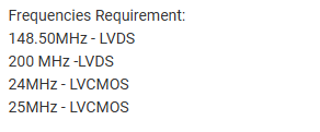
Frequencies Requirement:
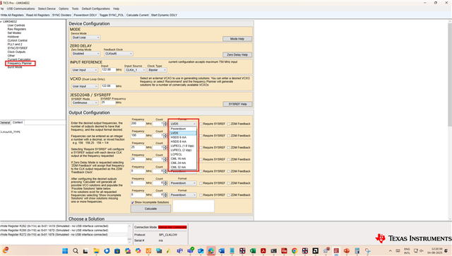
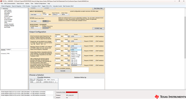
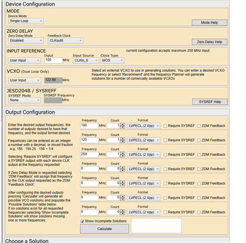
148.50MHz - LVDS
200 MHz -LVDS
24MHz - LVCMOS
25MHz - LVCMOS

Looking forward to the response.

Regards,
Dinesh

  • LMK04832-SEP is a phase locked loop that nominally requires a reference oscillator input, as opposed to an XO or equivalent which appears to be what you want. At this time, TI does not have any space-grade oscillators, we only have PLLs which require some reference oscillator input.

    Additionally, LMK04832-SEP has one common clock distribution path frequency, which is the source to all output dividers, and all output dividers are integer divide only. The least common multiple of the required outputs is 59.4GHz. The maximum supported clock distribution path frequency is 3.255GHz. There is no configuration of LMK04832-SEP which can simultaneously support all the required output frequencies. The minimum number of LMK04832-SEP required for the frequencies requested is two: one can generate 200MHz, 24MHz, and 25MHz from a 3GHz VCO, and the other can generate 148.5MHz from 2970MHz (divide-by-20 - there are other options but this one gives the best choice of reference frequencies). At least one reference oscillator input would be required as well, but it could be something standard like 10MHz or 100MHz. This reference could be cascaded from OSCin to OSCout of the first device, into OSCin of the second device, such that the application only requires one reference oscillator to generate all four frequencies.

  • In Frequency Planner Section of LMK04832, I can't able to select the CMOS in the format. I need to generate CMOS for my output requirement. Can you check and confirm this?

  • Hi Dinesh,

    Change the output format in clock outputs flex page.

    Pl3aaee note not all outputs support LVCMOS output.

    best regards,

    vicente

  • Hi Vicente,

    I have already changed the output format in Clock Output Page but in the Frequency Planner Page, CMOS Options are not there. I have checked the Evaluation Kit User Manual too. In that Frequency Planner Section is not there. Hereby, I attached the screenshot of that. Please check and let us know. Looking forward to the response.

    Regards,
    Dinesh

  • Hi Dinesh, 
    Yes but you don't need the CMOS option to appaer in the planner. 
    That planners main purpose is to ensure your frequency plan is possible to generate. 
    Ensure you can output the frequencies you want for example in my case: 

    I see a 3GHz VCO is one possible solution to this frequency plan and load the configuration. 

    I see the correct frequencies. 

    I can now go into each CLKoutx_FMT to change the output format. 

    This is register controlled. Editing these fields directly changes the registers if we had a device connected. It effectively writes to the registers via SPI. 

    Best regards, 

    Vicente 

  • Hi Vicente,

    Thank you for the information. 

    Regards,
    Dinesh

  • Hi,

    Can you suggest any Military Grade and Automotive Grade part with the same package and footprint of LMK04832?

    Regards,
    Dinesh

  • Hi,

    If I provide 3000MHz in VCO1, the PLL2 is not locked. Is there any issue because of this? Please check and confirm. Attached the screenshot for reference. Looking forward to the response.


    Regards,
    Dinesh

  • Hi Dinesh, 
    PLL2 isn't locked as N/R value * PFD ! = VCO frequency (3GHz) 

    There is a mathematical relationship between the VCO, and effecticely the PFD in this case. 

    In your case, you have a 122.88MHz PFD frequency the total N divider (taking into account the prescaler) is 24. 

    122.88MHz * 24 = 2949.12MHz 

    Please upload a clock tree of what your input clock is and desired outputs. 

    I see you uploaded this but in case somethings changed please include in your clock tree. 

    As Derek mentioned, this frequency plan specifically cannot be generated by the LMK04832-SP as the VCO coverage is limited from 2440MHz to 3255MHz. 
    Ensure the LCM of the outputs frequency you need falls under the VCO coverage range of the LMK04832-SP.

    Best regards, 

    Vicente 

  • Hi Vicente,

    Please find the Frequency Requirements and based on this, please provide the solution to Lock the PLL2.

    Frequency Requirement: 
    200MHz - LVDS
    100MHz - LVDS
    25MHz - LVCMOS
    24MHz - LVCMOS

    Looking forward to the response.

    Regards,
    Dinesh

  • Hi Dinseh, 
    What is your ref clk, is this a VCXO, XO, etc? 
    Do you plan on jitter cleaning or is your ref clk clean and you only want to operate in single loop (PLL2 only) mode which effectively acts as a clock generator? 

    I have created a config that assumes a 100MHz input with LMK04832 operating in single loop mode . 100MHzIn_SingleLoop_200_100_25_24MHzOut.tcs

    Best regards, 

    Vicente 

  • Hi Vicente,

    REFCLK = 100MHz/125MHz from XO.

    Looking for the single loop mode.

    Attached Clock File looks Ok for our requirements. Thank you for that.

    Regards,
    Dinesh

  • Hi Dinesh, 
    If utilizing a 100MHz XO - the config file is appropiate. 
    I will be closing this thread now - reach out again if you have any further questions. 

    Best regards, 

    Vicente 

  • Hi Vicente,

    Thank you for the information.

    Regards,
    Dinesh