LMK05318BEVM: Request for LMK05318BEVM Gerber Files for System Integration

Part Number: LMK05318BEVM
Other Parts Discussed in Thread: LMK05318B, , LMK05318, LMX2595

Tool/software:

Dear Texas Instruments Support Team,

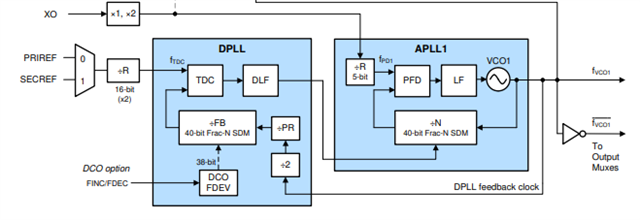
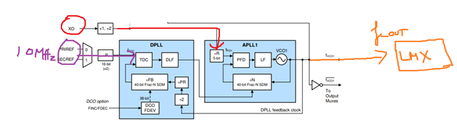
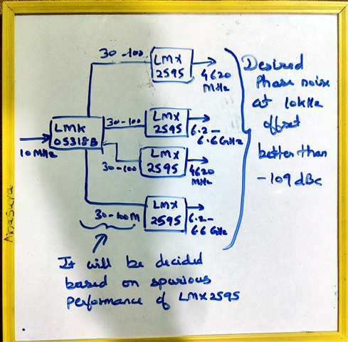
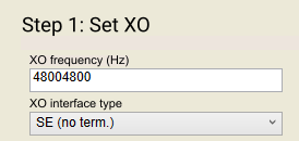
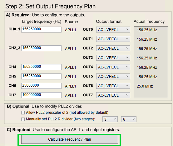
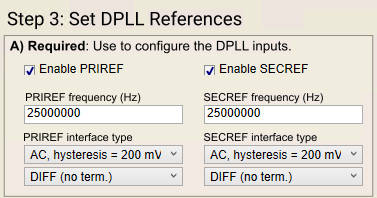
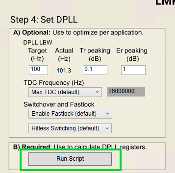
I am currently working on a high-performance clocking solution that incorporates the LMK05318B as the jitter cleaner and clock generator in my system. We are evaluating this part using the LMK05318BEVM evaluation module, and the results so far are very promising.

To ensure optimal layout for low-jitter performance in our custom design, we would like to refer to the original Gerber files or PCB layout of the LMK05318BEVM board as a reference for best practices in layout, impedance control, decoupling, and routing of differential clock signals.

We understand that these files may not be publicly available; however, if possible, we are willing to sign a Non-Disclosure Agreement (NDA) to gain access, solely for internal use and layout guidance.

Could you please let us know the process or requirements to obtain the Gerber or Altium files for the LMK05318BEVM?

Thank you very much for your support.

Best regards,

  • Hi Akshay,

    I don't have the board design files with me but I can look into it and get back.

    -Riley

  • Dear  Thank you for the response.

    Will be waiting for your update.

  • Hi Akshay,

    Here are design files. I'm also uploading these files to ti.com for future reference.

    -RileyLMK05318BEVM Altium Design Files.zipLMK05318BEVM Gerber Files.zip

  • Thank you for your response. I am planning to purchase the evaluation module to check if it works for low-phase-noise applications, an LO for the UP-Down converter. My system consists of LMX2595 as LO, which generates 4.6GHz, 6.2-6.6GHz, and the phase noise expected is below 109dBc at 10 KHz offset. When a direct reference is given from an OCXO CVHD950, I could meet the desired phase noise. Lmk05318b appears to be a good candidate for me to maintain the good phase noise of LMX2595. The reference frequency around 30-100 MHz would be generated based on spurious performance, also the system should be able to sync with an external clock of 10MHz on priority means LMK05318 has to sync. What do you suggest? Will this part help in my application? And also, I need a suggestion on a reference oscillator for lmk05318 at 10MHz, which has to be present in the absence of an external reference at second priority. 

    I am worried about products since I had already used HMC7044 from AD, which is similar, but the phase noise degraded when a reference was given through it.

    I read we have to be careful when feeding a reference from a PLL instead of OCXO, so will it serve my purpose?

  • Hi Akshay,

    LMK05318B can work with OCXO (through XO pins for APLL reference) in 30-100 MHz. When input reference become valid (PRIREF/SECREF pins), the device then can sync to these clocks through DPLL. In order to work in DPLL mode, the OCXO frequency needs to be in non-integer relation to BAW VCO1 2500 MHz. For example: 12.8 MHz, 19.2 MHz, 48 MHz, 38.88 MHz, etc.

    Reference input noise contribute to the outputs in a close-in jitter region. A typical jitter region is 12kHz-20MHz. XO (OCXO/TCXO) dominates noise <10kHz and REF noise dominates ~<100Hz depending on APLL and DPLL LBW which could also be optimized to narrow down to potentially filter input noise.

    -Riley

  • Thank you for the response. For me, it is compulsory to have 10 MHz as synchronization signal or reference to LMK on priority. The LMK out may be changed to the nearest non-integer value in the range 30- 100 MHz for LMX2595. Since I already explained to you my requirement, do you have any other part that I might have missed that would better fit the application?

  • So you need LMK05318B to provide input clock to LMX2595 instead of using OCXO CVHD950?

    LMK05318B could work here. LMK05318B can sync to 10 MHz through DPLL mode (using PRIREF/SECREF input), but in order to use DPLL mode, you'd need to choose XO input (XO/TCXO/OCXO) that has non-integer relation to BAW VCO1 2500 MHz as recommended above.

    In the absence of 10 MHz input, LMK05318B stays in holdover and the long term stability of holdover depends on the XO being used (OCXO > TCXO > XO). When 10 MHz is back valid, the device continue to sync to 10 MHz.

    -Riley

  • Thank you for your response, and I apologize for the delay in getting back to you.

    I understand that we need to use DPLL and ensure that the XO for APLL is non-integer for the VCBO output at 2500. I see the onboard XO is 48.0048 MHz in the EVAL board, which appears to be a general-purpose XO. Will this generate the desired phase noise results, or can you suggest any good OCXO/TCXO/XO, since I have had a bad experience with OCXO, as what they commit is not always observed in phase noise? The phase noise results shown in the white paper appear promising, as shown in the figure.

    ......

    Which XO or OCXO is used to get these results? And can I generate 4 different frequencies using dividers with the above configuration as a reference for four different LMX2595?

    Another question is that the external 10 MHz could be absent for a long duration, and phase noise is critical in application so in holdover for long time will phase noise be maintained without the external 10 MHz, and if not, can you suggest any XO/OCXO part to have as second priority on board 10 MHz to automatically switch to ?.

  • Hi Akshay,

    Which XO or OCXO is used to get these results?

    On EVAL board, it is TCXO 48.0048 MHz. The phase noise that we documented is often taken with XO being the signal generator SMA100B to show LMK05318B phase noise only. With a real XO/TCXO/OCXO, it would contribute noise in close-in region <10kHz.

    And can I generate 4 different frequencies using dividers with the above configuration as a reference for four different LMX2595?

    Technically, yes. But it depends on how many domains of these frequencies. Since the device has 2 VCOs, we could generate up to 2 domains. What are the frequencies needed? Do they all need to reference 10 MHz through DPLL? I can take a look to see if we have data taken with the TCXO.

    Another question is that the external 10 MHz could be absent for a long duration, and phase noise is critical in application so in holdover for long time will phase noise be maintained without the external 10 MHz, and if not, can you suggest any XO/OCXO part to have as second priority on board 10 MHz to automatically switch to ?.

    In the absence of 10 MHz input, the device enters holdover which allows the output clocks continue running without major disruption. For example, if XO has -1ppm and REF 10 MHz is 0 ppm. At start-up, output clock is at -1ppm because it references the XO. When the device locked to 10 MHz, the output is at 0 ppm. When REF 10 MHz is lost, the device enters holdover and the output maintains the ppm error of 0 ppm based on the history being accumulated during DPLL lock. Over long time holdover, it might drift away from 0ppm depending on TIE plot of the XO/TCXO/OCXO being used. When REF 10 MHz is back valid, device exists holdover and starts locking to REF 10 MHz at the ppm error of the input.

    You could also use XO/OCXO/TCXO to SECREF (assume the first 10 MHz is PRIREF). When PRIREF is lost and SECREF is valid, the device perform hitless switching allowing the output continue to run without changing in phase (phase cancellation) or gradually migrate to the new phase (phase slew control).

    -Riley

  • Thank you for the timely response. 

    The reference frequency would be decided based on spurious performance.

    For better visualization please refer the attached image of part of the system. Spurious below -75dBc desired after up down conversion, the mixer or up/dn module is not shown in below image.

    The input reference to lmx2595 although is written 30-100MHz, but we have to perform iterations for lowest spur and it will start from 20MHz. Mostly it should be between 20-40 MHz as I observed through formula given in lmx2595 datasheet. You may suggest if you have any better ideas for same.

    Since TI used signal generator, I wish to have recommendations on part number for 10MHz external and 48.004 MHz XO/OCXO.

  • Hi Akshay,

    Thanks for the diagram. We are looking into this and will reply in the coming days.

    Regards,

    Jennifer

  • Thank you for taking out time to look into this application. Will be waiting for the response.

  • Hi Akshay,

    Here is 50 MHz and 100 MHz taken with TXC TCXO 48 MHz and 48.0048 MHz (APLL mode). The 48MHz TCXO would provide less spurious on output phase noise.

    I don't have an OCXO 10 MHz to test with DPLL. But here is the 100 MHz phase noise with TXC TCXO 48.0048 MHz and 10 MHz from a signal generator to PRIREF to show you the close-in area where PRIREF contributes - this area is optimized through DPLL LBW. This data is at 100 Hz DPLL LBW. With a smaller DPLL LBW, input noise will be filtered out more.

    TXC TCXO used: 48 MHz - 7N48071001, 48.0048 MHz - 8W48070002

    Some OCXO that you can review: TXC OCXO OG48070101 (48 MHz), rakon Mercury+ series

    -Riley

  • Hi Riley

    Thank you for the response and detailed analysis.

    My understanding is that the phase noise results are for 100 MHz out with 48 MHz and 48.004 MHz TCXOs, from which the 48 MHz results appear better at a 100 Hz offset. Using a 10 MHz signal from a signal generator for the DPLL, the 100 MHz phase noise results look promising, and 100 Hz offset results can be improved using LBW tweeking.

    I feel I should get the eval board and check the results with both the TCXO and OCXO parts suggested by you, will also check the phase noise degradation, if any, in long time holdover, and then decide whether an extra 10 MHz TCXO/OCXO would be required. If you know a 10 MHz TCXO/OCXO that is compatible, then recommendations would be helpful.

  • Hi Akshay,

    You can review TCXO/OCXO family selection as listed in previous comment for 10 MHz.

    I will close this thread for now. Please reach out if you have questions regard configurating LMK05318B EVM.

    -Riley

  • Sure, thank you for the support and response.

  • Hi Riley

    I have placed the order for the evaluation board, but the part numbers you shared for  48 MHz and 48.004 MHz do not match the footprint on the evaluation board. You have also shared the results with these parts. May I know how you experimented?

  • Hi Akshay,

    8W48070002 is 48.0048 MHz XO - on the LMK05318B EVM

    7N48071001 is 48 MHz TCXO taken the data above, which is often bigger than XO due to higher performance.

    You could find XO 48 MHz in the same 2.5x2 footprint to replace the on-board 48.0048 MHz. Or you can use a signal generator provided to XO_P pin for a simple test.

    If you use other footprints, you'd need its own eval board to provide signal to XO and PRIREF of LMK05318B EVM.

    Best,

    Riley

  • Hi Riley,

    We have received the EVAL board, as discussed with DPLL disabled and internal XO used, the phase noise of LMX2595 is degrading, so I must use an external TCXO. The TCXO suggested by you is not available anywhere for purchase. Candefault settings_LMK05318B.tcs you please share a part number or series that could be available for purchase?

    Attached are the default settings of TICS pro used for testing with DPLL disabled, since we were not connecting PRIREF at this moment, but it would be required. 16 dBc degradation at 10 KHz offset for 6370 MHz out from LMX2595 with reference 100 MHz given from LMK05318Bevm.

  • Hi Akshay,

    NDK TCXO NT5032BD ENA5943A

    Epson TCXO TG-5510CA 80N 080N39FT

    I would recommend to test with a general input source (signal generator) for XO input at 48 MHz to ensure LMK05318B is proper configured and output is meeting the need before purchasing TCXO for further test.

    You'd need to set XO = 48 MHz, set output to 100 MHz and do Calculate frequency plan.

    Set Reference to 10 MHz and Run Script. It is ok to not have PRIREF/SECREF input at this moment, the device will not validate the input so DPLL is not attempting to lock.

    Do Write all regs and Soft-reset chip then check device status. The highlighted bits should be as shown for APLL mode lock and output is at correct frequency.

    Best,

    Riley