LMK04832: LDO bypass capacitors

Part Number: LMK04832
Other Parts Discussed in Thread: LMX2531

Tool/software:

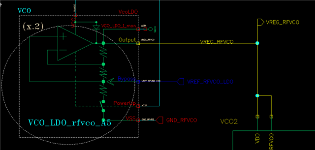
The datasheet shows 10uF and 0.1uF capacitors used for on-die LDO "bypassing".  No mention is made of the dielectric material for these capacitors.  If these capacitors are noise bypasses on an internal reference for the internal LDO's, then X5R and X7R with their piezoelectric effect will generate noise from vibration.  To avoid that vibration susceptibility film capacitors would be preferred for the 10uF (the 0.1uF can be COG).  If they locally bypass the supply to the internal regulator, then the external supply regulator can cope with that by servoing out vibration noise these capacitors would suffer.  Can it be clarified if these bypasses are for low noise filtering for the internal regulator reference,  or for internal regulator input supply?  

Thanks, 

Farron Dacus

  • LDObyp1 is on the output of the VCO LDO. LDObyp2 is on the feedback node.

    I think in the same way that the external regulator can servo out noise to the LDO inputs, the internal LDO can servo out noise on its own output to some extent. I don't have any data to back this up, so take with a grain of salt, but my impression from other similar devices is that you normally get 50 to 70 dB PSRR from these higher-current internal regulators, and the PSRR of internal LDOs tends to decline rapidly past ~1MHz. But I suspect most piezoelectric issues are at frequencies well below 1MHz. My suggestion is, unless you can trace some system spur back to a specific vibration source coupled through an LDObyp1 cap, there's likely no need to resort to alternate dielectrics.

    Since the 0.1µF on LDObyp2 is connected directly to the LDO feedback node, it should definitely be C0G whenever possible. Care should be taken in the layout to avoid running other high current traces below this node.

    This is something the datasheet should document. Right now we're in the process of making revisions to the LMK04832 datasheet, so I'll pass this along to the reviewer for inclusion in the next revision.

  • Hello Derek:

    Thanks for the prompt response and the useful information.  

    OK, with LDObyp1 being the output of the LDO, a high dielectric constant piezo electric capacitor like X5R or X7R is fine. They are standard practice in that role because the microphonic noise is generally less than 3kHz, and the bandwidth of the regulator loop greater than 100kHz, so that noise is suppressed by the feedback action of the regulator.  

    I'm not so sure that the 0.1uF is on the "feedback node", because in the absence of gain relative to the reference node the feedback node is the same as the output node.  And, if there is gain relative to a reference voltage, such as to gain a 1.2V bandgap voltage up to a more useful level, putting a capacitor on that node is introducing RC phase shift in the feedback loop that takes it closer to instability.   

    So, it would seem more likely that the 0.1uF is actually on the reference of the regulator feedback loop.  That reference needs to be low noise in order for the regulator output to be low noise.  For example, an on die resistor of 50k (from bandgap output to regulator reference node) and an external 0.1uF on the reference would have an RC corner of 32Hz. This reduces bandgap reference noise above that frequency so that the output has lower noise than the raw bandgap reference, and that output suppresses vibration noise on the output capacitance as well.  

    And, if that 0.1uF is on the reference node, then it needs to be non-microphonic, because any vibration noise on that node will be carried straight to the output.  And, if there is gain from reference to output, then any vibration noise on the reference is actually gained up on the output.  

    ...Farron

  • Just to be certain, here's a small snippet of the top-level of the LDO schematic. The node VREG_RFVCO is tied to the LDObyp1 pin, and the VREF_RFVCO_LDO node is tied to the LDObyp2 pin. The connection is directly on the reference node as you describe, rather than the feedback node. So thanks for pushing back on that, you're correct.

    Internally, the resistance between + and - inputs is very small (a few tens of ohms) with a bias current of around 1.5mA running through that net, which appears to be correcting for base mismatch in the difference amplifier. VREF_RFVCO_LDO is tuned to about 1.5V, and the servo adds around 1V on top of the reference to the VREGG_RFVCO node. It seems like noise on the reference node just moves the output by an equivalent amount, and there shouldn't be any significant gain in this path. Nevertheless, the servo still adds around 1V on top of any in-band noise coupled onto this output, suggesting a need for non-microphonic external bypass capacitance.

    I also followed along the history of the design, all the way back to the LMX2531 from which it was more or less copied. Several of the apps engineers from that time recall there were some customer issues with microphonic noise coupling into the VCO LDO, though none of us recall any more specific details. There's one other person I'd like to ask internally who's very knowledgeable about LDO design, but they're out of office this week - I'll update with more info when possible.

    Unless I learn something surprising about this design next week, I still stand by the C0G recommendation for the 0.1µF on LDObyp2.

  • Derek, thanks very much for detailed presentation.  Yes, we'll be going with 0.1uF COG on that LDObyp2 pin.