Tool/software:
Good evening,
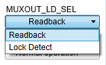
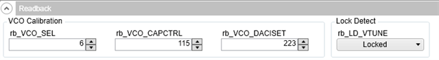
I am having difficulty getting our LMX2572 to show Lock Detect as 1 either through the readback or via the pin. Reading the registers back, all values are as expected with the exception of the following regs:
r112: wrote 0x0000, returned status value 0xFEEC
r111: wrote 0x0000, returned status value 0x01B7
r110: wrote 0x0600, returned status value 0x0719
r109: wrote 0x0000, returned bad value 0x3800
r108: wrote 0x0000, returned bad value 0x00A1
r107: wrote 0x0000, returned bad value 0x8801
I would expect regs 110-112 to read back as non-zero values because these are status regs, but I can't rationalise why they would be these values. For instance, I would expect r110 [4:0] to be all 0's based on the datasheet.
Additionally, I did not expect r107-109 to have non-zero values. Is this normal?
My config regs are below. We are using a custom board.
Thanks
R125 0x7D2288
R124 0x7C0000
R123 0x7B0000
R122 0x7A0000
R121 0x790000
R120 0x780000
R119 0x770000
R118 0x760000
R117 0x750000
R116 0x740000
R115 0x730000
R114 0x727802
R113 0x710000
R112 0x700000
R111 0x6F0000
R110 0x6E0600
R109 0x6D0000
R108 0x6C0000
R107 0x6B0000
R106 0x6A0007
R105 0x694440
R104 0x6809C4
R103 0x670000
R102 0x660000
R101 0x650000
R100 0x6409C4
R99 0x630000
R98 0x620000
R97 0x610000
R96 0x600000
R95 0x5F0000
R94 0x5E0000
R93 0x5D0000
R92 0x5C0000
R91 0x5B0000
R90 0x5A0000
R89 0x590000
R88 0x580000
R87 0x570000
R86 0x560000
R85 0x550000
R84 0x540001
R83 0x53FFFF
R82 0x52FFFF
R81 0x510000
R80 0x500000
R79 0x4F0000
R78 0x4E00CF
R77 0x4D0000
R76 0x4C000C
R75 0x4B0800
R74 0x4A0000
R73 0x49003C
R72 0x480175
R71 0x47004D
R70 0x46C350
R69 0x450000
R68 0x4403E8
R67 0x430000
R66 0x4201F4
R65 0x410000
R64 0x401388
R63 0x3F0000
R62 0x3E00AF
R61 0x3D00A8
R60 0x3C000A
R59 0x3B0000
R58 0x3A6401
R57 0x390020
R56 0x380000
R55 0x370000
R54 0x360000
R53 0x350000
R52 0x340421
R51 0x330080
R50 0x320080
R49 0x314180
R48 0x3003E0
R47 0x2F0300
R46 0x2E07F2
R45 0x2DCE3C
R44 0x2C01C3
R43 0x2B0000
R42 0x2A0000
R41 0x290000
R40 0x280000
R39 0x270001
R38 0x260000
R37 0x250305
R36 0x240028
R35 0x230004
R34 0x220010
R33 0x211E01
R32 0x2005BF
R31 0x1FC3E6
R30 0x1E18A6
R29 0x1D0000
R28 0x1C0488
R27 0x1B0002
R26 0x1A0808
R25 0x190624
R24 0x18071A
R23 0x17007C
R22 0x160001
R21 0x150409
R20 0x147048
R19 0x1327B7
R18 0x120064
R17 0x1100EC
R16 0x100080
R15 0x0F060E
R14 0x0E1820
R13 0x0D4000
R12 0x0C5008
R11 0x0BB018
R10 0x0A1378
R9 0x090004
R8 0x082000
R7 0x0700B2
R6 0x062802
R5 0x0528C8
R4 0x040A43
R3 0x030782
R2 0x020500
R1 0x010808
R0 0x006298