CDCE6214-Q1: Input Clock Format

Part Number: CDCE6214-Q1
Other Parts Discussed in Thread: CDCE6214

Tool/software:

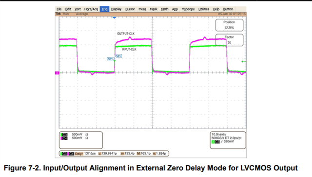
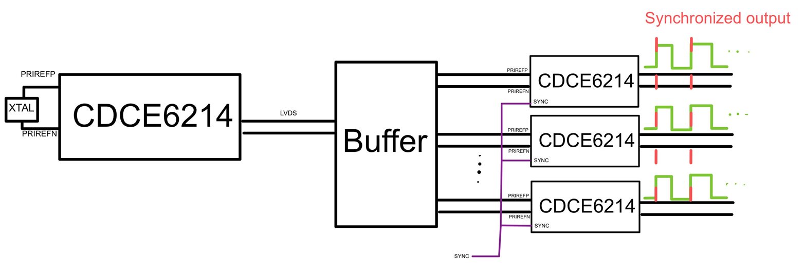
Hello, I am attempting to synchronize multiple of this device and I am thinking on using another CDCE6214-Q1 to create this reference clock signal into PRIREF_P and PRIREF_N (and of course feed a SYNC pulse to all devices). My question is if it would be feasable to use the LVDS output AC-coupled directly into all the other CDCE6214-Q1s PRIREF_P and PRIREF_N pins, or if the input has to be a sinusoidal or something else. Thank you.

  • Felipe,

    Are you trying to just synchronize the outputs to each other, or synchronize the outputs to an unput?

    There is a SYNC function through either I2C or pin control that allows synchronizing the outputs to each other. For alignment between the input and the output, you need to set up Zero-Delay Mode (ZDM).

    Thanks,

    Kadeem

  • Hey Kadeem,

    I am trying to synchronize all outputs, but to my understanding all clocks need a common clock and sync signal. My question was if I can use a buffered output from another CDCE6214 as the clock input source for the rest.

    Thank you!,

    Felipe

  • Felipe,

    You can edge-align the outputs from one CDCE6214 to another CDCE6214 by leveraging the zero-delay mode. A reference clock is provided on PRIREF as the PFD reference, and either SECREF (external ZDM) or OUT2 (internal ZDM, higher propagation delay) is used as the feedback clock. This behavior is described on pages 20 and 21 of the datasheet.

    Is there any reason why you are using multiple CDCE6214 for synchronization instead of a single buffer device? Do you have a clock tree that I can use as a reference for better understanding of your requirements?

    Thanks,

    Kadeem

  • Hey Kadeem,

    I apologize for not being very clear with my question. I have multiple CDCE6214s which I want their outputs to be syncrhonized. My question was regarding the signal that I would input into each of the CDCE6214s into PRIREF (as opposed to using crystals on each one). My question is then, can I take the output of another clock (like a CDCE6214), buffer its output, and use the buffered signals into each PRIREF pins? See attached image for visual explanation:

    Thank you,

    Felipe

  • Felipe,

    Understood, much clearer now.

    For multiple CDCE6214, this may not work the way that you desire due to the skew from device to device. The SYNC timing is not exact - the number of VCO cycles for SYNC to be achieved my differ from device to device.

    How many output clocks do you need, and are these LVDS or a different format? The best solution may be to use an oscillator with a single buffer device for achieving synchronization between all of the outputs.

    Thanks,
    Kadeem