LMK1D1204: Design Review

Part Number: LMK1D1204

Tool/software:

Hello,

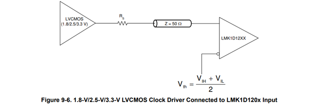
I am using a single-ended LVCMOS clock with a 3.3V amplitude as the input. Please find the attached schematic for reference. I have a few questions regarding the biasing configuration.

Current Setup:

  • The LVCMOS clock signal (3.3V) is AC coupled to the positive input pin, IN0_P.

  • The unused negative input pin, IN0_N, is to be biased at the recommended half-supply voltage of 1.65V.

  • Questions:
    1. Since the positive input (IN0_P) is AC coupled, do I also need to provide a DC bias to it? If yes, what should be the resistor value?

    2. Is a voltage divider required to bias the unused input pin IN1_N at 1.65V, or is another method acceptable?

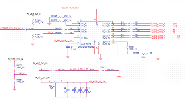
Attached is the schematic above. Please review and let me know if this correct?

  • Hello Misba, 
    Yes, bias _P side to VCC/2 
    I recommend 1k resistors for reduced current draw. 

    Normally an LVCMOS clock is already biased - if possible do not AC couple i.e. remove C3. 

    Best regards, 

    Vicente 

  • Hello,

    I have a query on the Bias_P and N side. 

    • Bias_P side connected to VCC/2:
      If capacitor C3 is removed because the LVCMOS clock is already biased, then what is the purpose of the voltage divider circuit that connects to VCC/2?

    • Bias_N side in the schematic:
      Please confirm if the biasing arrangement at IN0_N is correct. Since the N-side is not being used, why is biasing necessary? Why can’t it be simply grounded through a capacitor?

  • Hi Misba,

    Assuming your LVCMOS input is already biased, there is no purpose for the voltage divider if C3 is removed. That divider circuit becomes redundant.

    The current arrangement does not appear correct, as IN0_N appears to be floating. Biasing is required on the N side because that pin needs to be held at the midpoint of the swing of the P input. It would be sufficient to AC couple that pin to GND if the P input were AC coupled, but AC coupling the input without a bias could damage the receiver of this device, which is rated for an absolute minimum value of -0.3V. 

    Back to the 3.3V LVCMOS signal, which should swing from 0V up to 3.3V. It's bias level is 3.3V/2 = 1.65V. The IN0_N input needs to be held at this same voltage for the device to operate as expected.

    Thanks,

    Michael